ホーム インターフェイス LVDS、M-LVDS、PECL の各 IC

SN55LVRA4-SEP

プレビュー

クワッド チャネル高速差動レシーバ

製品詳細

Function Receiver Protocols LVDS Number of transmitters 0 Number of receivers 4 Supply voltage (V) 3.3 Signaling rate (Mbps) 400 Input signal CMOS, ECL, LVCMOS, LVDS, LVECL, LVPECL, PECL Output signal LVTTL Rating Space Operating temperature range (°C) -55 to 125
SOIC (D) 16 59.4 mm² 9.9 x 6
  • VID V62/25606-01XE
  • Total ionizing dose characterized at 30krad (Si)
    • Total ionizing dose radiation lot acceptance testing (TID RLAT) for every wafer lot to 30krad (Si)
  • Single-event effects (SEE) characterized:
    • Single event latch-up (SEL) immune to linear energy transfer (LET) = 50MeV-cm2 /mg
    • Single event transient (SET) characterization report available
  • 400Mbps signaling rate
  • Operates with a single 3.3V supply
  • –4V to 5V extended common-mode input voltage range
  • Differential input thresholds < ±50mV with 50mV of hysteresis over entire common-mode input voltage range
  • Complies with TIA/EIA-644 (LVDS)
  • Active fail-safe assures a high-level output with no input and input remains high-impedance on power down
  • Bus-pin ESD protection exceeds 15kV HBM
  • TTL control inputs are 5V tolerant
  • Space enhanced plastic (SEP)
    • Controlled baseline
    • Gold wire, NiPdAu lead finish
    • One assembly and test site, one fabrication site
    • Extended product life cycle
    • Military (–55°C to 125°C) temperature range
    • Product traceability
    • Meets NASA ASTM E595 outgassing specification

The SN55LVRA4-SEP offers the widest common-mode input voltage range in the industry. These receivers provide an input voltage range specification compatible with a 5V PECL signal as well as an overall increased ground-noise tolerance.

The SN55LVRA4-SEP include a failsafe circuit that provides a high-level output within 60ns after loss of the input signal. The most common causes of signal loss are disconnected cables, shorted lines, or powered-down transmitters. The failsafe circuit prevents noise from being received as valid data under these fault conditions.

The intended application and signaling technique of these devices is point-to-point baseband data transmission over controlled impedance media of approximately 100Ω. The transmission media can be printed-circuit board traces, backplanes, or cables. The ultimate rate and distance of data transfer is dependent upon the attenuation characteristics of the media and the noise coupling to the environment.

The SN55LVRA4-SEP is characterized for operation from –55°C to 125°C.

ダウンロード 字幕付きのビデオを表示 ビデオ

技術資料

star =TI が選定したこの製品の主要ドキュメント
結果が見つかりませんでした。検索条件をクリアしてから、再度検索を試してください。
4 をすべて表示
種類 タイトル 最新の英語版をダウンロード 日付
* データシート SN55LVRA4-SEP Radiation Tolerant Quad Channel High-Speed Differential Receiver データシート (Rev. A) PDF | HTML 2025年 12月 5日
* 放射線と信頼性レポート SN55LVRA4-SEP Single-Event Effects (SEE) Radiation Report PDF | HTML 2025年 12月 8日
* 放射線と信頼性レポート SN55LVRA4-SEP Production Flow and Reliability Report PDF | HTML 2025年 11月 12日
セレクション・ガイド TI Space Products (Rev. K) 2025年 4月 4日

設計および開発

その他のアイテムや必要なリソースを参照するには、以下のタイトルをクリックして詳細ページをご覧ください。

評価ボード

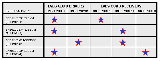
SN65LVDS31-33EVM — 評価モジュール、SN65LVDS31/SN65LVDS33 用

TI offers a series of low-voltage differential signaling (LVDS) evaluation modules (EVMs) designed for analysis of the electrical characteristics of LVDS drivers and receivers. Four unique EVMs are available to evaluate the different classes of LVDS devices offered by TI.

As seen in the Combination (...)

ユーザー ガイド: PDF
シミュレーション・モデル

SN65LVDS33 IBIS Model (Rev. A)

SLLC069A.ZIP (6 KB) - IBIS Model
シミュレーション・ツール

PSPICE-FOR-TI — TI Design / シミュレーション ツール向け PSpice®

PSpice® for TI は、各種アナログ回路の機能評価に役立つ、設計とシミュレーション向けの環境です。設計とシミュレーションに適したこのフル機能スイートは、Cadence® のアナログ分析エンジンを使用しています。PSpice for TI は無償で使用でき、アナログや電源に関する TI の製品ラインアップを対象とする、業界でも有数の大規模なモデル ライブラリが付属しているほか、選択された一部のアナログ動作モデルも利用できます。

設計とシミュレーション向けの環境である PSpice for TI を使用すると、内蔵のライブラリを使用して、複雑なミックスド (...)
シミュレーション・ツール

TINA-TI — SPICE ベースのアナログ・シミュレーション・プログラム

TINA-TI は、DC 解析、過渡解析、周波数ドメイン解析など、SPICE の標準的な機能すべてを搭載しています。TINA には多彩な後処理機能があり、結果を必要なフォーマットにすることができます。仮想計測機能を使用すると、入力波形を選択し、回路ノードの電圧や波形を仮想的に測定することができます。TINA の回路キャプチャ機能は非常に直観的であり、「クイックスタート」を実現できます。

TINA-TI をインストールするには、約 500MB が必要です。インストールは簡単です。必要に応じてアンインストールも可能です。(そのようなことはないと思いますが)

TINA は DesignSoft (...)

ユーザー ガイド: PDF
英語版 (Rev.A): PDF
パッケージ ピン数 CAD シンボル、フットプリント、および 3D モデル
SOIC (D) 16 Ultra Librarian

購入と品質

記載されている情報:
  • RoHS
  • REACH
  • デバイスのマーキング
  • リード端子の仕上げ / ボールの原材料
  • MSL 定格 / ピーク リフロー
  • MTBF/FIT 推定値
  • 使用原材料
  • 認定試験結果
  • 継続的な信頼性モニタ試験結果
記載されている情報:
  • ファブの拠点
  • 組み立てを実施した拠点

推奨製品には、この TI 製品に関連するパラメータ、評価基板、またはリファレンス デザインが存在する可能性があります。

サポートとトレーニング

TI E2E™ フォーラムでは、TI のエンジニアからの技術サポートを提供

コンテンツは、TI 投稿者やコミュニティ投稿者によって「現状のまま」提供されるもので、TI による仕様の追加を意図するものではありません。使用条件をご確認ください。

TI 製品の品質、パッケージ、ご注文に関するお問い合わせは、TI サポートをご覧ください。​​​​​​​​​​​​​​

ビデオ