SLVA927A November 2017 – April 2019 LM25066A , LM25066I , LM5050-1 , LM5051 , LM5064 , LM5066 , LM5067 , LM5069 , LM66100 , LM74500-Q1 , LM74700-Q1 , TPL7407LA , TPS1H100-Q1 , TPS1HA08-Q1 , TPS2113A , TPS2115A , TPS22810 , TPS22915 , TPS22916 , TPS22918 , TPS22971 , TPS22990 , TPS23525 , TPS2412 , TPS24751 , TPS24770 , TPS25942A , TPS2595 , TPS2660 , TPS27S100 , TPS2H160-Q1 , TPS4H160-Q1 , ULN2003A
A Power Switch provides an electrical connection from a voltage source or ground to a load. It saves power across multiple voltage rails and protects subsystems from damage. It also provides enhanced component protection, inrush current protection, and minimizes printed-circuit board (PCB) size.
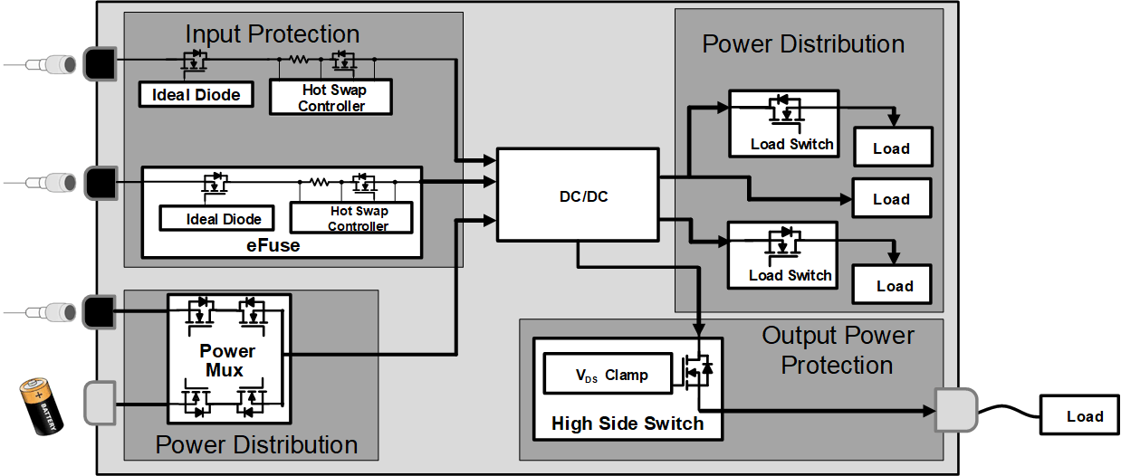
There are several power switch topologies with different functions that address different applications. Load Switches establish the power switch foundation by providing safe and reliable distribution of power. Applications typically using load switches include power distribution, power sequencing, inrush current control, and reduced current leakage. Integrated Power MUX devices are similar to load switches but allow for multiple input sources. This set of electronic switches is used to select and transition between two or more input power paths to a single output while also providing input power protection.
eFuses and Hot Swap controllers provide additional input power path protection functions such as current sense monitoring, current limiting, undervoltage and overvoltage protection, and thermal shutdown. This makes these devices ideal for hot-plug and transient events that would otherwise damage system components. These benefits help reduce system maintenance costs and maximize equipment uptime.
Ideal diode, ORing controllers provide protection against reverse-polarity conditions by monitoring an external FET, significantly reducing power loss, and blocking reverse current. Whenever a transient event occurs, the controller monitors and adjusts the external FET to prevent damage to upstream components.
Smart high-side switches are for off-board load protection. They provide additional diagnostic telemetry that monitors the output load current and detects short-circuit and open-load events. Smart high-side switches have adjustable current limits, allowing for more reliable integration into applications with either large inrush current startup profiles or low peak currents. Adding a smart high-side switch to a design leads to a smarter and more robust solution for driving capacitive, inductive, and LED loads.
Low-side switches connect the load to ground instead of providing a connection between a power supply and the load. By including an integrated flyback diode, low-side switches help eliminate inductive load transients by dissipating current in a circular loop. This allows them to drive inductive loads such as solenoids, relays, and motors.
This application report highlights the different topologies within the power switch portfolio, and provides suggestions in choosing the correct solution for a faster design time.
POWER DISTRIBUTION | POWER PATH PROTECTION | ||||||
---|---|---|---|---|---|---|---|
Load Switch | Power MUX
(2 input, 1 output) |
eFuse (Internal FET) | Hot Swap (External FET)
|
Ideal Diode
ORing Controller |
Smart High-Side Switch | Low-Side Switch | |
Voltage Range | 0 V to 18 V | 2.8 V to 22 V | 2.7 V to 60 V | ±80 V | ±75 V | 6 V to 40 V | 0 V to 100 V |
Max Operating Current | 15 A | 4.5 A | 15 A | N/A | N/A | 12 A | 1 A |
Functions | |||||||
Inrush Current Control | ✓ | ✓ | ✓ | ✓ | ✓ | ||
Adjustable Current Limit | ✓ | ✓ | ✓ | ✓ | |||
Reverse Current Blocking | ✓ | ✓ | ✓ | ✓ | ✓ | ||
Current Sense Monitoring | ✓ | ✓ | ✓ | ||||
Short-Circuit Protection | ✓(1) | ✓ | ✓ | ✓ | ✓ | ||
Overvoltage Protection | ✓ | ✓ | ✓ | ||||
Reverse Polarity Protection | ✓ | ✓ | ✓ | ✓ | ✓ | ||
Power Good Signal | ✓ | ✓ | ✓ | ||||
Inductive Load Compatibility | ✓ | ✓ | |||||
Load-Dump Compatibility | ✓ | ✓ | ✓ | ✓ | ✓ | ||
Thermal Shutdown | ✓ | ✓ | ✓ | ✓ | ✓ |
All trademarks are the property of their respective owners.
Integrated load switches are electronic switches that turn power rails on and off. When the internal FET turns on, current flows from the input to output and passes power to the downstream circuitry. When the device is enabled, the rise time of the output voltage (VOUT) can be controlled by adjusting the capacitance on an external pin (CT pin). When the device is disabled, the fall time of VOUT is controlled through the quick output discharge (QOD). QOD pulls the output to ground whenever the device is turned off, preventing the output from floating or entering an undetermined state.
Some common functions of load switches include power savings, power sequencing, and inrush current control. Power savings is important in applications looking to minimize current dissipation and maximize power efficiency. By disconnecting the supply from a load or subsystem, the switch minimizes power drawn from inactive loads. Power sequencing is important in applications where individual voltage rails need to be turned on and off in a specific order. By configuring the CT and QOD pins, the ramp-up and power-down timing can be adjusted. Inrush current control protects systems that contain large bulk capacitors near the load. When power is initially applied to the system, charging these capacitors can result in a large inrush current that exceeds the nominal load current. If left unaddressed, this can cause voltage rails to fall out of regulation due to the drop, resulting in the system entering an undesired state. Load switches can mitigate the inrush current by using the CT pin to manage the rise time of the power rail. This leads to a linear output slew rate with no voltage dips or external regulators required.
DESCRIPTION | DEVICES | VOLTAGE RANGE | MAX CURRENT | TYPICAL Ron | PACKAGE |
---|---|---|---|---|---|
Adjustable rise time, adjustable QOD | TPS22918 | 1 V to 5.5 V | 2 A | 52 mΩ | SOT |
TPS22810 | 2.7 V to 18 V | 2 A | 79 mΩ | SOT | |
Space-constrained applications | TPS22915 | 1.05 V to 5.5 V | 2 A | 37 mΩ | CSP |
TPS22916 | 1 V to 5.5 V | 2 A | 60 mΩ | CSP | |
Self protected with controlled rise time | TPS22919 | 1.6 V to 5.5 V | 1.5 A | 90 mΩ | SOT |
Lowest ON-resistance, power good indication | TPS22990 | 1 V to 5.5 V | 10 A | 3.9 mΩ | SON |
Fast turn-on time (≤ 65 µs), Power Good indication, QOD, thermal shutdown | TPS22971 | 0.65 V to 3.6 V | 3 A | 6.7 mΩ | DSBGA |
Integrated Power MUX devices allow a system to transition between different power sources seamlessly. If the main power supply fails, power multiplexing allows the system to switch to a backup power supply, such as a battery, to preserve operating conditions. Power multiplexing can also provide switching between two different voltage levels for subsystems that operate at two different voltages. In this scenario, to prevent reverse current flow from VOUT into one of the VIN channels, reverse current protection (RCP) blocks current from flowing back through the body diode. Power multiplexing also contains adjustable current limits. If the current exceeds the threshold set by the switch, the switch clamps the channel and prevent current from exceeding the limit. Furthermore, if the current limit forces the device to reach higher temperatures, thermal shutdown turns off the switch until it can operate at safe conditions again. Similar to load switches, power MUX switches also contain inrush current control to prevent large transient current events.
Power MUX devices can switch between different power rails in three general ways: manually, automatically, or both. Manual switchovers occur with an external GPIO. Whenever you want to switch between power rails, the enable pin is toggled and the output is powered by the other power rail. Automatic switchover occurs whenever the primary power supply fails or is disconnected. When the device detects the voltage drop, it automatically switches to the backup power rail. There are some Power MUX solutions which offer the flexibility to be used in an automatic configuration and to be controlled by a manual control signal. This method can have a default (automatic) priority, but can then be overridden by an external microcontroller if needed.
DESCRIPTION | DEVICE | RECOMMENDED VOLTAGE RANGE | MAX CURRENT | TYPICAL Ron | PACKAGE |
---|---|---|---|---|---|
Automatic priority and manual override, adjustable current limit | TPS2120 | 2.8 V to 22 V | 3 A, each channel | 62 mΩ | CSP |
Automatic priority and manual override, fast output switchover, adjustable current limit | TPS2121 | 2.8 V to 22 V | 4.5 A, each channel | 56 mΩ | QFN |