SNVAA13 December 2020 LM117HVQML-SP , LM117QML-SP , TPS7H5001-SP , UC1823A-SP , UC1825-DIE , UC1825-SP , UC1825A-DIE , UC1825A-SP , UC1825B-SP , UC1842-SP , UC1842A-SP , UC1843-SP , UC1843A-DIE , UC1843A-SP , UC1843B-SP , UC1844-SP , UC1844A-SP , UC1845-SP , UC1845A-SP , UC1846-SP , UC1856-SP , UC1863-SP
Application Brief
Controlling Input Power for Present and Next-Generation Power Controllers
With the adoption of electric propulsion as well as the rapid increase in the throughput of modern satellites, power supply designers are faced with the issue of addressing the ever-increasing load currents. To help minimize the impact of these higher load currents on the overall satellite power architecture, design engineers have a number of different options, such as increasing the voltage power distribution buses (e.g. 28 V to 50 V) or considering the adoption of space saving GaN FET technology. In this article, I will focus on the primary power block of the satellite which typically use a pulse width modulation (PWM) controller, typically one of the highest wattage power supplies in the satellite, and will outline a few alternative approaches to powering it.
RC Approach
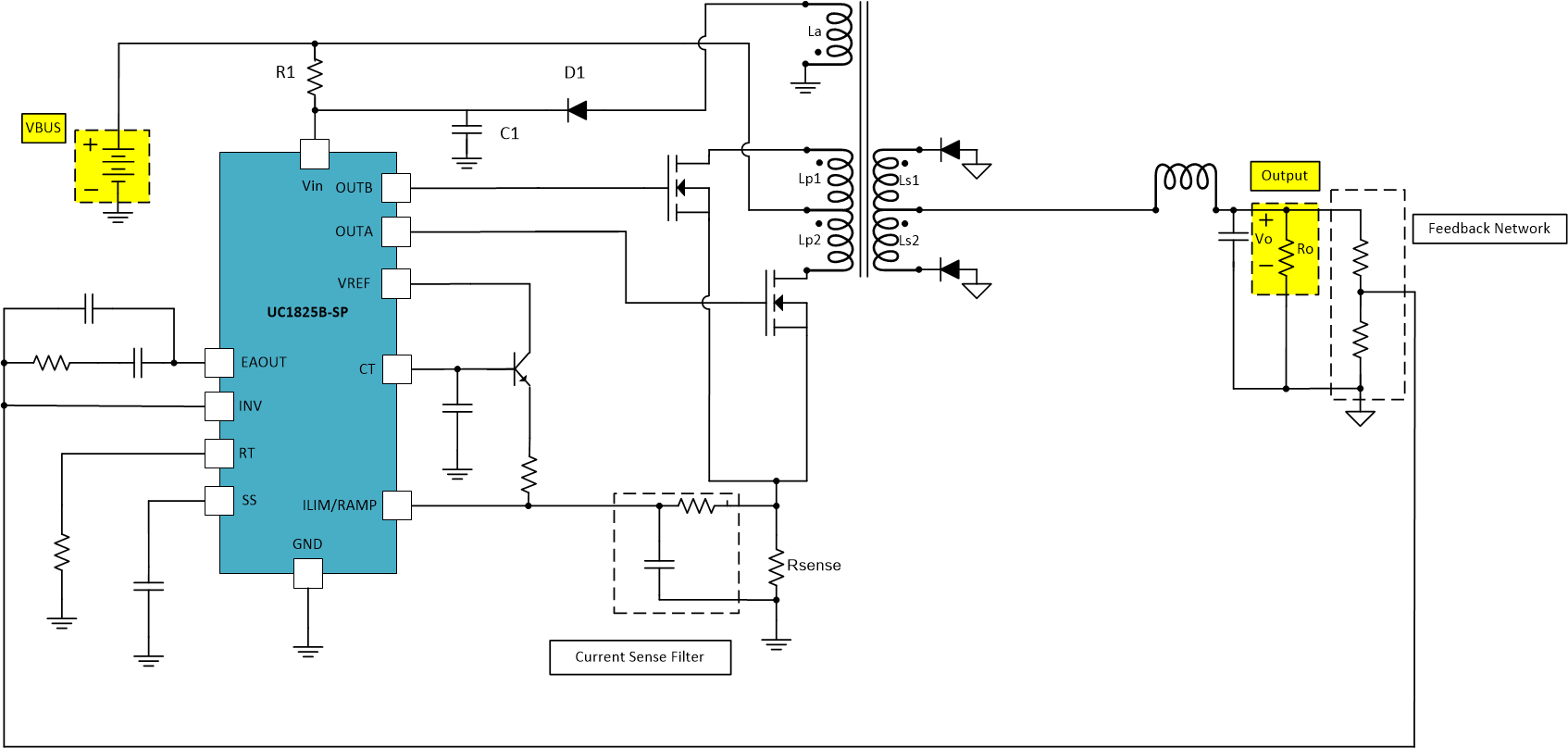
In many isolated power supply designs, the PWM controller is powered by the auxiliary winding through the power stage transformer Figure 1-1. This technique is designed to keep the overall system efficiency as high as possible. In this example, during normal operation the auxiliary winding, D1 and C1 components provide power to the UC1825B-SP, a radiation-hardness-assured (RHA), dual-output PWM controller. During startup, the resistor R1 trickle charges C1 from the input supply rail. The C1 capacitor holds up the supply voltage (VCC) long enough for the controller to start switching the power MOSFET gate, which is powered via the auxiliary winding.
 Figure 1-1 50-V Isolated DC/DC Power
Supply Design with Resistor Based Start-Up Circuit
Figure 1-1 50-V Isolated DC/DC Power
Supply Design with Resistor Based Start-Up CircuitLinear Regulator Approach
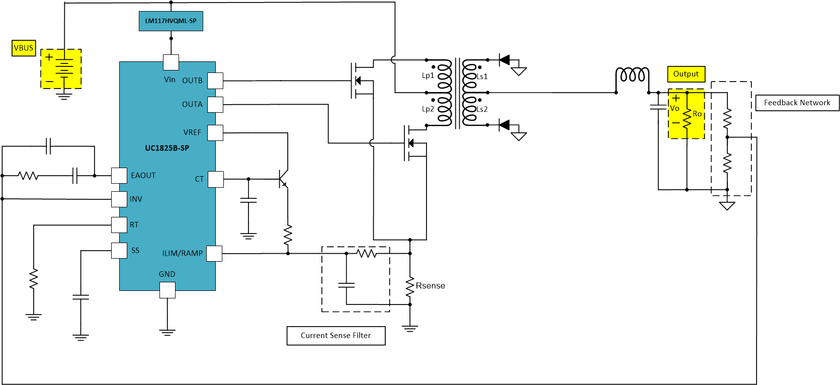
The circuit in Figure 1-2 replaces the R1 resistor and the auxiliary winding with the LM117HVQML-SP, a 60-V RHA linear regulator.
 Figure 1-2 50-V Isolated DC/DC Power
Supply Design with a Linear Regulator
Figure 1-2 50-V Isolated DC/DC Power
Supply Design with a Linear RegulatorBy using a linear regulator, designers can achieve a much lower input capacitance to the controller and can achieve around 2% accuracy at the output. The RC startup circuit is unregulated and thus may require a Zener diode to set a maximum voltage. This voltage can dip depending on the conditions of the controller, which makes it difficult to set a minimum operating voltage over all worst case conditions. A stable and predictable voltage is particularly important for newer controllers that may have much tighter VCC tolerance requirements. These next-generation controllers are specifically optimized to support gallium nitride (GaN) FET technology, which holds the promise of both even smaller designs and higher efficiency.
Comparison of Both Aproaches
To compare the different circuits we have outlined the options and estimated power consumption of the different approaches in Table 1-1. For this example, we will assume a nominal 50-V input voltage. When factoring in the input voltage tolerances, we assumed a voltage range swing from 40 V to 60 V. For this example the VCC of the UC1825B-SP controller is set at 12 V and the auxiliary winding will output 14 V at 40 V and increase to 21 V at 60 V due to the nature of the transformer. Let’s assume the startup current to be 2 mA and the quiescent current of the LM117HVQML-SP to be 1.2 mA.
| Configuration | Estimated Power Consumption Based on 40-V to 60-V Voltage Range | Comment |
|---|---|---|
| RC Approach: R1 trickle charging C1 during startup then the auxiliary winding power the rest of time | 0.5 W to 0.8 W | Depending on the selection of the R1 & C1 values, this approach results in a larger board area footprint but also the lowest power consumption |
| R1 powering the PWM controller directly without the auxiliary winding | 1.3 W to 3.4 W | Highest power over input voltage conditions and unregulated supply rail variations |
| LM117HVQML-SP powering the PWM controller without the auxiliary winding | 1.4 W to 2.0 W | Tighter regulation, faster start-up, smaller board area footprint but slightly higher power consumption |
Conclusion
While the first and third architectures in the table have substantial merit, the RC circuit is the most efficient. There is a concern the circuit may become unstable in light load conditions, which prevent the auxiliary winding from charging the capacitor. However, light load conditions are not very common in most space applications. If the condition does exist then the alternative linear regulator approach could address the potential instability of the RC approach. The linear regulator approach does consume more power but is unique in that it provides a much more precise output voltage, which will enable the designer to consider newer generation controller/FET architectures.
Alternate Device Recommendations
Depending on the necessary system requirements, there may be additional devices that provide alternative functionality. If an isolated flyback topologies is preferred then only single outputs are required and the PWM controller UC1843B-SP might be considered. If the input voltage of isolated power supply is less than 40 V then the linear regulator the LM117QML-SP is better suited. See Table 1-2.
| Device | Optimized Parameter | Performance Trade-Off |
|---|---|---|
| UC1834B-SP | Single output more optimized for flyback topologies with similar radiation performance | Does not support dual-output push-pull topology |
| LM117QML-SP | Input range 4.2 V to 40 V offering numerous package options with similar radiation performance | Reduced input voltage range |