-
TPS7B4250-Q1 低压降电压跟踪 LDO
DATA SHEET
TPS7B4250-Q1 低压降电压跟踪 LDO
本资源的原文使用英文撰写。 为方便起见,TI 提供了译文;由于翻译过程中可能使用了自动化工具,TI 不保证译文的准确性。 为确认准确性,请务必访问 ti.com 参考最新的英文版本(控制文档)。
1 特性
- 适用于汽车电子 应用
- 符合 AEC-Q100 标准的下列结果
- -20V 至 45V 宽范围、最大输入电压范围
- 输出电流,50mA
- 极低输出跟踪容限,
5mV(最大值) - 当 IOUT = 10mA 时,低压降电压为 150mV
- 组合基准和使能输入
- 轻负载时,40µA 的低静态电流
- 极端、宽 ESD 范围。
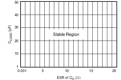
- 与 1µF 至 50µF 陶瓷输出电容器,1mΩ 至 20Ω 等效串联电阻 (ESR) 一同使用时保持稳定
- 反极性保护
- 过热保护
- 对接地和电源的输出短路保护
- SOT-23 封装
2 应用
- 电路板外传感器电源
- 高精度电压跟踪
3 说明
TPS7B4250-Q1 器件是一款单片、集成型低压降跟踪器。此器件采用 SOT-23 封装。TPS7B4250-Q1 器件被设计用来为汽车环境中的电路板外传感器供电。此集成电路 (IC) 具有针对过载、过热、反向极性和电池与接地输出短路的集成保护功能。
调节输入引脚 ADJ 上施加的基准电压用于对高达 VIN = 45V 的电源电压进行稳压,负载电流高达 50mA。
通过将调节/使能输入引脚 (ADJ/EN) 置为低电平,TPS7B4250-Q1 器件可切换至待机模式,从而最大限度地降低静态电流。
器件信息(1)
| 器件型号 | 封装 | 封装尺寸(标称值) |
|---|---|---|
| TPS7B4250-Q1 | SOT-23 (5) | 2.90mm x 1.60mm |
- 如需了解所有可用封装,请见数据表末尾的可订购产品附录。
4 修订历史记录
Changes from A Revision (November 2013) to B Revision
- Changed HBM ESD 分类等级,从 2 改为 3A Go
- Changed CDM ESD 分类等级,从 C4 改为 C6Go
- Added 引脚配置和功能部分,ESD 额定值表,特性 描述部分,器件功能模式,应用和实施部分,电源相关建议部分,布局部分,器件和文档支持部分以及机械、封装和可订购信息部分Go
- Deleted the transient current and 107-pF capacitor for HBM table notes from the ESD Ratings table Go
- Changed input voltage symbol from VIN to VI for the ΔVO(ΔVI) and Vdropout parameters and the output voltage symbol from VOUT to VO for the IL parameter in the Electrical Characteristics tableGo
- Added IO and CO to the PSRR test condition in the Electrical Characteristics table Go
- Changed the max value for Vdropout where IO = 10 mA from 250 to 265 in the Electrical Characteristics tableGo
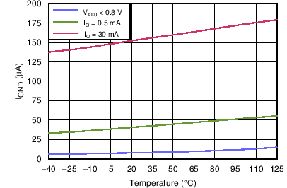
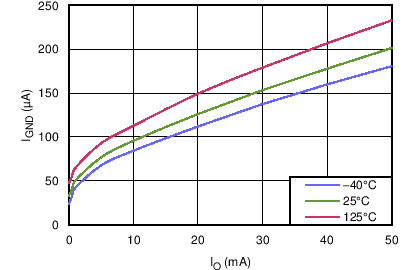
- Deleted the VADJ = 5 V condition for the Ground current vs Temperature graph and changed the legendGo
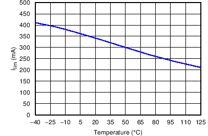
- Changed the y axis units from mV to mA in the Current-limit vs Temperature graph Go
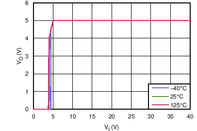
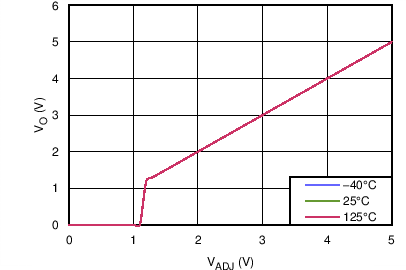
- Added the VADJ condition statement to the Input Voltage vs Output Voltage graph and changed the y-axis from IO to VOGo
- Changed the title of Figure 8 from Input Voltage vs Output Voltage to Reference Voltage vs Output Voltage, and changed the y-axis from IO to VO. Also added the VI condition statement to the graphGo
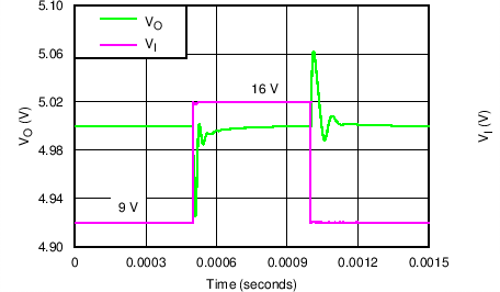
- Changed the second y axis from IO to VI and removed the units in the Line TransientGo
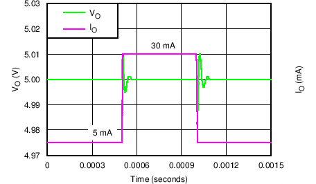
- Deleted the units from the second y axis in the Load TransientGo
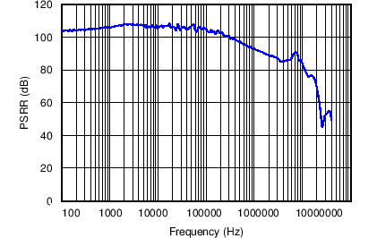
- Added the VADJ condition statement to the Power-supply Rejection Ratio vs Frequency graphGo
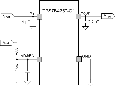
- Added resistor-divider values to the Tracking LDO With Enable Circuit figureGo
Changes from * Revision (October 2013) to A Revision
- Changed CDM ESD 分类等级,通篇从 C3B 改为 C4Go
- Changed VOUT min value from –0.3 to –1 in the Absolute Maximum Ratings tableGo
- Added transient current flow to ESD rating in the Absolute Maximum Ratings tableGo
- Changed HBM absolute maximum rating from 2 kV to 4 kVGo
- Deleted relevant ESR value from Recommended Operating Conditions tableGo
- Added grater-than-or-equal-to (≥) value to VADJ/EN in condition statement of the Electrical Characteristics table Go
- Added VADJ = 1.5 V to both test conditions for VUVLO parameter in the Electrical Characteristics tableGo
- Changed max value for load regulation parameter from 3 to 4 in the Electrical Characteristics tableGo
- Changed max value for the current consumption test condition where IO = 0.5 mA from 80 to 90 in the Electrical Characteristics tableGo
- Added the Detailed Description sectionGo
- Added the TPS7B4250 block diagramGo
5 Pin Configuration and Functions
DBV Package
5-Pin SOT-23
Top View

Pin Functions
| PIN | TYPE | DESCRIPTION | |
|---|---|---|---|
| NAME | NO. | ||
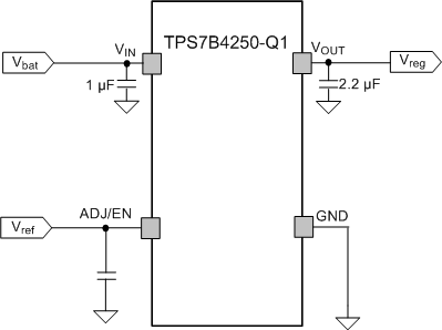
| ADJ/EN | 1 | I | This pin connects to the reference voltage. A low signal disables the IC and a high signal enables the IC. Connected the voltage reference directly or with a voltage divider for lower output voltages. To compensate for line influences, TI recommends to place a capacitor close to the IC pins. |
| GND | 2 | G | Internally connected to pin 5 |
| 5 | Internally connected to pin 2 | ||
| VIN | 3 | I | This pin is the IC supply. To compensate for line influences, TI recommends to place a capacitor close to the IC pins. |
| VOUT | 4 | O | VOUT is an external capacitor that is required between VOUT and GND with respect to the capacitance and ESR requirements given in the Recommended Operating Conditions. |
6 Specifications
6.1 Absolute Maximum Ratings
over operating free-air temperature range (unless otherwise noted)(1)| MIN | MAX | UNIT | |||
|---|---|---|---|---|---|
| Input voltage, unregulated input, VIN(2)(3) | –20 | 45 | V | ||
| Output voltage, regulated output, VOUT | –1 | 22 | V | ||
| Adjust input and enable input voltage, ADJ/EN(2)(3) | –0.3 | 22 | V | ||
| ADJ Voltage minus input voltage (ADJ–VIN), VIN > 0 V | 7 | V | |||
| Operating junction temperature, TJ | –40 | 150 | °C | ||
| Storage temperature, Tstg | –65 | 150 | °C | ||
(1) Stresses beyond those listed under absolute maximum ratings may cause permanent damage to the device. These are stress ratings only and functional operation of the device at these or any other conditions beyond those indicated under recommended operating conditions is not implied. Exposure to absolute-maximum-rated conditions for extended periods may affect device reliability.
(2) All voltage values are with respect to ground, GND.
(3) Absolute maximum voltage.
6.2 ESD Ratings
| VALUE | UNIT | |||
|---|---|---|---|---|
| V(ESD) | Electrostatic discharge | Human-body model (HBM), per AEC Q100-002(1) | ±4000 | V |
| Charged-device model (CDM), per AEC Q100-011 | ±1000 | |||
(1) AEC Q100-002 indicates that HBM stressing shall be in accordance with the ANSI/ESDA/JEDEC JS-001 specification.
6.3 Recommended Operating Conditions
over operating free-air temperature range (unless otherwise noted)(2)| MIN | MAX | UNIT | ||
|---|---|---|---|---|
| VIN | Unregulated input | 4 | 40 | V |
| VOUT | regulated output | 1.5 | 18 | V |
| ADJ/EN | Adjust input and enable input voltage | 1.5 | 18 | V |
| ADJ–VIN | ADJ voltage minus input voltage | 5 | V | |
| COUT | Output capacitor requirements(1) | 1 | 50 | µF |
| ESRCOUT | Output ESR requirements | 0.001 | 20 | Ω |
| TJ | Operating junction temperature | –40 | 150 | °C |
(1) The minimum output capacitance requirement is applicable for a worst-case capacitance tolerance of 30%.
(2) Within the functional range, the IC operates as described in the circuit description. The electrical characteristics are specified within the conditions given in the related electrical characteristics table.
6.4 Thermal Information
| THERMAL METRIC(2)(1) | TPS7B4250-Q1 | UNIT | |
|---|---|---|---|
| DBV (SOT-23) | |||
| 5 PINS | |||
| RθJA | Junction-to-ambient thermal resistance | 171.7 | °C/W |
| RθJC(top) | Junction-to-case (top) thermal resistance | 81.1 | °C/W |
| RθJB | Junction-to-board thermal resistance | 31.7 | °C/W |
| ψJT | Junction-to-top characterization parameter | 4.5 | °C/W |
| ψJB | Junction-to-board characterization parameter | 31.2 | °C/W |
| RθJC(bot) | Junction-to-case (bottom) thermal resistance | N/A | °C/W |
(1) The thermal data is based on the JEDEC standard high K profile, JESD 51-7. Two-signal, two-plane, four-layer board with 2-oz. copper. The copper pad is soldered to the thermal land pattern. Also, correct attachment procedure must be incorporated.
(2) For more information about traditional and new thermal metrics, see the Semiconductor and IC Package Thermal Metrics application report, SPRA953.
6.5 Electrical Characteristics
VI = 13.5 V, 18 V ≥ VADJ/EN ≥ 1.5 V, TJ = –40ºC to 150ºC unless otherwise stated| PARAMETER | TEST CONDITIONS | MIN | TYP | MAX | UNIT | |
|---|---|---|---|---|---|---|
| VUVLO | VIN undervoltage detection | Ramp up VI until the output turns on, VADJ = 1.5 V | 3.65 | V | ||
| Ramp down VI until the output turns off, VADJ = 1.5 V | 3 | |||||
| ΔVO | Output-voltage tracking accuracy | IO = 100 µA to 1 mA, VI = 4 V to 40 V, 1.5 V < VADJ < VI – 0.3 V | –4 | 4 | mV | |
| IO = 1 mA to 50 mA, VI = 4 V to 40 V, 1.5 V < VADJ < VI – 1.5 V | –5 | 5 | ||||
| ΔVO(ΔIL) | Load regulation steady-state | IO = 1 mA to 30 mA | 4 | mV | ||
| ΔVO(ΔVI) | Line regulation steady-state | IO = 10 mA, VI = 6 V to 40 V | 3 | mV | ||
| PSRR | Power-supply ripple rejection | Frequency = 100 Hz, Vrip = 0.5 VPP, IO = 5 mA, CO = 2.2 µF | 60 | dB | ||
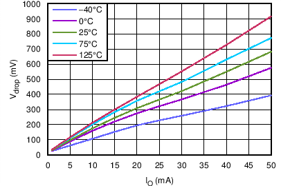
| Vdropout | Dropout voltage, Vdropout = VI – VQ | IO = 10 mA, VI ≥ 4 V(1) | 150 | 265 | mV | |
| IO = 50 mA, VI ≥ 4 V(1) | 550 | 1000 | ||||
| IL | Output-current limitation | VO short to GND | 100 | 500 | mA | |
| IR | Reverse current at VIN | VI = 0 V, VO = 20 V, VADJ = 5 V | –5 | 0 | µA | |
| IRN1 | Reverse current at negative input voltage | VI = –20 V, VO = 0 V, VADJ = 5 V | –5 | 0 | µA | |
| IRN2 | VI = –20 V, VO = 20 V, VADJ = 5 V | –5 | 0 | |||
| TSD | Thermal shutdown temperature | TJ increasing because of power dissipation generated by the IC | 175 | °C | ||
| IQ | Current consumption | VADJ < 0.8 V, TA ≤ 85°C(2) | 7.5 | 15 | µA | |
| VADJ < 0.8 V, TA ≤ 125°C | 20 | |||||
| IO = 0.5 mA, VADJ = 5 V | 40 | 90 | ||||
| IO = 30 mA, VADJ = 5 V | 150 | 350 | ||||
| IADJ | Adjust-input and enable-input current | VADJ = 5 V | 1 | µA | ||
| VADJ,low | Adjust and enable low signal valid | VO = 0 V | 0.8 | V | ||
| VADJ,high | Adjust and enable high signal valid | |VO – VADJ| < 5 mV | 1.5 | 18 | V | |
(1) Measured when the output voltage VQ has dropped 10 mV from the typical value.
(2) Ensured by design.
6.6 Typical Characteristics

| VI = VADJ = 4 V | IO = 10 mA | |
| VI = 13.5 V | VADJ = 5 V | |
| VI = VADJ = 4 V | ||
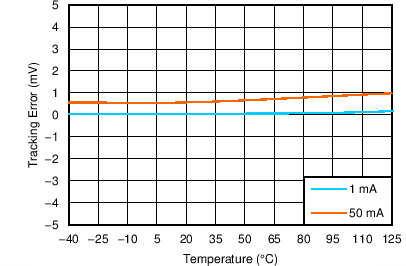
| VI = 13.5 V | VADJ = 5 V | IO = 1 mA, 50 mA |
