• Menu
  • Product
  • Email
  • PDF
  • Order now
  • High-Voltage to Low-Voltage DC-DC Converter Reference Design With GaN HEMT

    • TIDT403A August   2024  – December 2024


  • CONTENTS
  • SEARCH
  • High-Voltage to Low-Voltage DC-DC Converter Reference Design With GaN HEMT
  1.   1
  2.   Description
  3.   Features
  4.   Applications
  5. 1Test Prerequisites
    1. 1.1 Voltage and Current Requirements
    2. 1.2 Required Equipment
    3. 1.3 Considerations
    4. 1.4 Dimensions
  6. 2Testing and Results
    1. 2.1 Efficiency Graphs
    2. 2.2 Efficiency Data
    3. 2.3 Thermal Performance
    4. 2.4 Bode Plots
    5. 2.5 Light Load Efficiency Optimization
    6. 2.6 Switching Frequency Choice
  7. 3Waveforms
    1. 3.1 Switching
    2. 3.2 Output Voltage Ripple
    3. 3.3 Overcurrent Protection
    4. 3.4 Load Transients
    5. 3.5 Turn ON and OFF
  8. 4References
  9.   Trademarks
  10. IMPORTANT NOTICE
search No matches found.
  • Full reading width
    • Full reading width
    • Comfortable reading width
    • Expanded reading width
  • Card for each section
  • Card with all content


Test Report

High-Voltage to Low-Voltage DC-DC Converter Reference Design With GaN HEMT

Description

This reference design describes a 3.5kW high-voltage to low-voltage DC-DC converter with 650V Gallium nitride (GaN) high-electron mobility transistors (HEMT). Using LMG3522R030 as primary switches makes the converter work at a high switching frequency. In this design, the converter uses a smaller size transformer. To ease the thermal performance of active clamping metal-oxide semiconductor field-effect transistors (MOSFETs), the converter uses two-channel active clamping circuits.

Features

  • GaN based phase-shifted full-bridge (PSFB) using LMG3522 and controlled using C29 microcontroller unit (MCU)
  • 200kHz switching frequency, magnetic size is 35% less than 100kHz
  • 95.48% at 200kHz, 400V Vin, 13.5V Vout, about 1kW
  • Dual active clamping circuits for high-frequency scenario and low synchronous rectifier (SR) MOSFET voltage stress
  • Light load efficiency optimization promotes maximum 5% efficiency

Applications
  • Hybrid, electric, and powertrain systems
  • DC/DC converter system
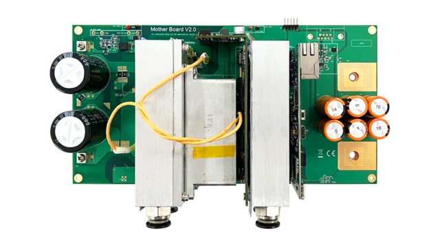
PMP41078 Top View of BoardTop View of Board
PMP41078 Bottom View of BoardBottom View of Board
PMP41078 Block Diagram Block Diagram


Texas Instruments

© Copyright 1995-2025 Texas Instruments Incorporated. All rights reserved.
Submit documentation feedback | IMPORTANT NOTICE | Trademarks | Privacy policy | Cookie policy | Terms of use | Terms of sale