How to Measure Ripple for Better Design Outcomes
George Lakkas
Testing switching power supplies includes many different tests, one of them being the output-voltage peak-to-peak ripple. Output-voltage ripple is the alternating current (AC) component of the direct current (DC) output voltage. It’s generated by a combination of factors, including the output capacitor’s equivalent series resistance (ESR), the voltage drop across the output capacitance, duty cycle and switching frequency.
Because it impacts the overall voltage tolerance of the rail, the peak-to-peak output-voltage ripple is a target specification in many processor, field-programmable gate array (FPGA), application-specific integrated circuit (ASIC) and system-on-chip (SoC) data sheets and design guides.
How you measure the ripple can affect your ability to meet the design requirements.
Figure 1 shows a typical output-voltage ripple probe setup.
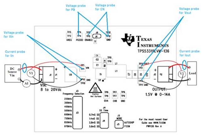 Figure 1 Output-voltage Ripple Probe
Setup
Figure 1 Output-voltage Ripple Probe
SetupProbing using a clip-on probe shows an increased ripple that may be partly the result of the ground-wire loop picking up noise, as shown in Figure 2.
 Figure 2 Output Voltage Ripple Probe
with a Clip-on Probe and Ground Wire Fully Extended, Picking up Noise from the
Nearby Switch Node
Figure 2 Output Voltage Ripple Probe
with a Clip-on Probe and Ground Wire Fully Extended, Picking up Noise from the
Nearby Switch NodeProbing using the pigtail method improves ripple, even though the tip is again near the switch node, as Figure 3 shows. The ground loop is much shorter; thus the noise pickup is less severe.
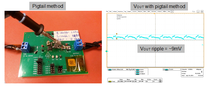 Figure 3 Output-voltage Ripple Probe
Using the Pigtail Method; the Probe Ground Is in Contact with the Pigtail, Which
Is Connected to the Board Ground
Figure 3 Output-voltage Ripple Probe
Using the Pigtail Method; the Probe Ground Is in Contact with the Pigtail, Which
Is Connected to the Board GroundUsing a coaxial cable method improves results even more, as Figure 4 shows. Directly soldering the woven copper shield on the board ground minimizes the ground loop further.
 Figure 4 Output-voltage Ripple Probe
Using Coaxial Method
Figure 4 Output-voltage Ripple Probe
Using Coaxial MethodFigure 5 shows a close-up of the coaxial cable.
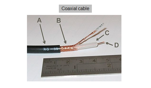 Figure 5 Coaxial Cable Close-up: the
Outer Plastic Sheath (a); Woven Copper Shield (Ground) (b); Inner Dielectric
Insulator (c); and Copper Core (vOUT) (d)
Figure 5 Coaxial Cable Close-up: the
Outer Plastic Sheath (a); Woven Copper Shield (Ground) (b); Inner Dielectric
Insulator (c); and Copper Core (vOUT) (d)Another similar measurement method is to use a probe jack like that shown in Figure 6. The outside jacket is the ground connected directly on the board while allowing the probe tip to connect to the voltage test point.
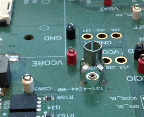 Figure 6 Probe Jack
Of all of these methods, using a differential probe is probably the best way to measure ripple accurately. It can eliminate the ground-loop noise pickup error, especially when connecting other electronic equipment to the same board ground (such as electronic loads and multimeters).
Figure 7 shows the two test points for differential probe connections on the board.
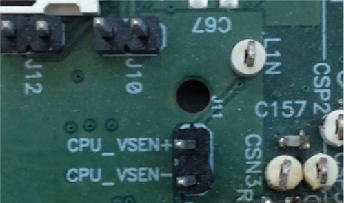 Figure 7 Differential Probe Test Points
CPU_VSEN+ and CPU_VSEN-
Figure 7 Differential Probe Test Points
CPU_VSEN+ and CPU_VSEN-If you are trying to meet tight output-voltage regulation requirements and have a low peak-to-peak voltage-ripple target, how you measure the ripple on your board can make you or break you. Optimizing your probe method will help you with your measurements and meet the specifications. Practice and compare any of the probe methods discussed in this post on a switching regulator evaluation module (EVM) like the TPS40304EVM-353. As well, read the application report, “Output Ripple Voltage for Buck Switching Regulator” and understand how ripple voltage is calculated and reported in WEBENCH® Power Designer.
IMPORTANT NOTICE AND DISCLAIMER
TI PROVIDES TECHNICAL AND RELIABILITY DATA (INCLUDING DATASHEETS), DESIGN RESOURCES (INCLUDING REFERENCE DESIGNS), APPLICATION OR OTHER DESIGN ADVICE, WEB TOOLS, SAFETY INFORMATION, AND OTHER RESOURCES “AS IS” AND WITH ALL FAULTS, AND DISCLAIMS ALL WARRANTIES, EXPRESS AND IMPLIED, INCLUDING WITHOUT LIMITATION ANY IMPLIED WARRANTIES OF MERCHANTABILITY, FITNESS FOR A PARTICULAR PURPOSE OR NON-INFRINGEMENT OF THIRD PARTY INTELLECTUAL PROPERTY RIGHTS.
These resources are intended for skilled developers designing with TI products. You are solely responsible for (1) selecting the appropriate TI products for your application, (2) designing, validating and testing your application, and (3) ensuring your application meets applicable standards, and any other safety, security, or other requirements. These resources are subject to change without notice. TI grants you permission to use these resources only for development of an application that uses the TI products described in the resource. Other reproduction and display of these resources is prohibited. No license is granted to any other TI intellectual property right or to any third party intellectual property right. TI disclaims responsibility for, and you will fully indemnify TI and its representatives against, any claims, damages, costs, losses, and liabilities arising out of your use of these resources.
TI’s products are provided subject to TI’s Terms of Sale (www.ti.com/legal/termsofsale.html) or other applicable terms available either on ti.com or provided in conjunction with such TI products. TI’s provision of these resources does not expand or otherwise alter TI’s applicable warranties or warranty disclaimers for TI products.
Mailing Address: Texas Instruments, Post Office Box 655303, Dallas, Texas 75265
Copyright © 2023, Texas Instruments Incorporated