-
LM53603-Q1 (3 A), LM53602-Q1 (2 A) 3.5 V to 36 V Wide-VIN Synchronous 2.1 MHz Step-Down Converters for Automotive Applications SNVSA42B June 2015 – May 2016 LM53602-Q1 , LM53603-Q1
PRODUCTION DATA.
-
LM53603-Q1 (3 A), LM53602-Q1 (2 A) 3.5 V to 36 V Wide-VIN Synchronous 2.1 MHz Step-Down Converters for Automotive Applications
- 1 Features
- 2 Applications
- 3 Description
- 4 Revision History
- 5 Device Comparison Table
- 6 Pin Configuration and Functions
- 7 Specifications
- 8 Detailed Description
- 9 Application and Implementation
- 10Power Supply Recommendations
- 11Layout
- 12Device and Documentation Support
- 13Mechanical, Packaging, and Orderable Information
- IMPORTANT NOTICE
LM53603-Q1 (3 A), LM53602-Q1 (2 A) 3.5 V to 36 V Wide-VIN Synchronous 2.1 MHz Step-Down Converters for Automotive Applications
1 Features
-
The LM53603-Q1, LM53602-Q1 are available as AEC-Q1-Qualified Automotive Grade Products With Following Results:
- Device Temperature Grade 1: -40°C to +125°C Ambient Operating Range
- Device HBM ESD Classification Level 1C
- Device CDM ESD Classification Level C4B
- 3 A or 2 A maximum load current
- Input Voltage Range from 3.5 V to 36 V: Transients to 42 V
- Output Voltage Options: 5 V, 3.3 V, ADJ
- 2.1 MHz Fixed Switching Frequency
- ±2% Output Voltage Tolerance
- –40°C to 150°C Junction Temperature Range
- 1.7 µA Shutdown Current (typical)
- 24 µA Input Supply Current at No Load (typical)
- No external Feed-back Divider Required for 5 V or 3.3 V output
- Reset Output With Filter and Delay
- Automatic Light Load Mode for Improved Efficiency
- User-Selectable Forced PWM mode (FPWM)
- Built-in Loop Compensation, Soft-start, Current Limit, Thermal Shutdown, UVLO, and External Frequency Synchronization
- Thermally Enhanced 16-lead Package:
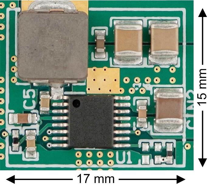
5 mm x 4.4 mm x 1 mm
2 Applications
- Navigation/GPS
- Instrument Cluster
- ADAS, Infotainment, HUD
3 Description
The LM53603-Q1, LM53602-Q1 buck regulators are specifically designed for automotive applications, providing an output voltage of 5 V or 3.3 V (with ADJ option) at 3 A or 2 A, from an input voltage of up to 36 V. Advanced high-speed circuitry allows the device to regulate from an input of up to 20 V, while providing an output of 5 V at a switching frequency of 2.1 MHz. The innovative architecture allows the device to regulate a 3.3 V output from an input voltage of only 3.5 V. All aspects of this product are optimized for the automotive customer. An input voltage range up to 36 V, with transient tolerance up to 42 V, eases input surge protection design. An open drain reset output, with filtering and delay, provides a true indication of system status. This feature negates the requirement for an additional supervisory component, saving cost and board space. Seamless transition between PWM and PFM modes, along with a no-load operating current of only 24 µA, ensures high efficiency and superior transient response at all loads.
Device Information(1)
| PART NUMBER | PACKAGE | BODY SIZE (NOM) |
|---|---|---|
| LM53603-Q1 LM53602-Q1 |
HTSSOP (16) | 5.00 mm x 4.40 mm |
- For all available packages, see the orderable addendum at the end of the data sheet.
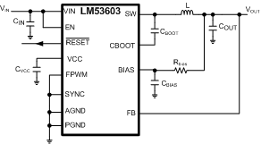
Simplified Schematic

Automotive Power Supply with 5 V, 3 A Output

4 Revision History
Changes from A Revision (June 2015) to B Revision
- Added Automotive Features Go
- changed representation of RESET threshold for clarity (physical parameter unchanged)Go
- added CFF recommendation table for ADJ version Go
- Corrected saturation current for some of the recommended inductors in the table "Recommended Inductors" Go
- Added recommendation for CVCC: use of X7R component is highly recommended Go
- Added Cboot recommended rating of 10V in the CBOOT section Go
- added power dissipation curve for 5Vout and 3.3Vout Go
- added layout recommendation for CVCC and CBIAS Go
Changes from * Revision (June 2015) to A Revision
5 Device Comparison Table
| PART NUMBER | PACKAGE | MAXIMUM OUTPUT CURRENT |
|---|---|---|
| LM53603-Q1 | HTSSOP (16) | 3 A |
| LM53602-Q1 | HTSSOP (16) | 2 A |
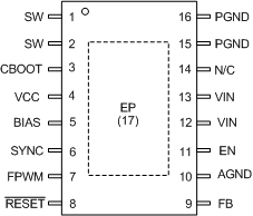
6 Pin Configuration and Functions

Pin Functions
| PIN | I/O(1) | DESCRIPTION | |
|---|---|---|---|
| NAME | NO. | ||
| SW | 1,2 | P | Regulator switch node. Connect to power inductor. Connect pins 1 and 2 directly together at the PCB. |
| CBOOT | 3 | P | Bootstrap supply input for gate drivers. Connect a high quality 470 nF capacitor from this pin to SW. |
| VCC | 4 | O | Internal 3.15 V regulator output. Used as supply to internal control circuits. Do not connect to any external loads. Can be used as logic supply for control inputs. Connect a high quality 3.3 µF capacitor from this pin to GND. |
| BIAS | 5 | P | Input to internal voltage regulator. Connect to output voltage point. Do not ground. Connect a high quality 0.1 µF capacitor from this pin to GND. |
| SYNC | 6 | I | Synchronization input to regulator. Used to synchronize the regulator switching frequency to the system clock. When not used connect to GND; do not float. |
| FPWM | 7 | I | Mode control input to regulator. High = forced PWM (FPWM). Low = auto mode; automatic transition between PFM and PWM. Do not float. |
| RESET | 8 | O | Open drain reset output. Connect to suitable voltage supply through a current limiting resistor. High = power OK. Low = fault. RESET will go low when EN = low. |
| FB | 9 | I | Feedback input to regulator. Connect to output voltage sense point for fixed 5 V and 3.3 V output. Connect to feedback divider tap point for ADJ option. Do not float or ground. |
| AGND | 10 | G | Analog ground for regulator and system. All electrical parameters are measured with respect to this pin. Connect to EP and PGND on PCB. |
| EN | 11 | I | Enable input to the regulator. High = ON. Low = OFF. Can be connected directly to VIN. Do not float. |
| VIN | 12, 13 | P | Input supply to the regulator. Connect a high quality bypass capacitor(s) from this pin to PGND. Connect pins 12 and 13 directly together at the PCB. |
| N/C | 14 | - | This pin has no connection to the device. |
| PGND | 15, 16 | G | Power ground to internal low side MOSFET. Connect to AGND and system ground. Connect pins 15 and 16 directly together at the PCB. |
| EP | 17 | G | Exposed die attach paddle. Connect to ground plane for adequate heat sinking and noise reduction. |