-
LP5562 Four-Channel RGB- or White-LED Driver With Internal Program Memory and Independent Channel Control
- 1 Features
- 2 Applications
- 3 Description
- 4 Revision History
- 5 Pin Configuration and Functions
-
6 Specifications
- 6.1 Absolute Maximum Ratings
- 6.2 ESD Ratings
- 6.3 Recommended Operating Conditions
- 6.4 Thermal Information
- 6.5 Electrical Characteristics
- 6.6 Logic Interface Characteristics
- 6.7 Recommended External Clock Source Conditions
- 6.8 I2C Timing Requirements (SDA, SCL)
- 6.9 Typical Characteristics: Current Consumption
- 6.10 Typical Characteristics: LED Output
-
7 Detailed Description
- 7.1 Overview
- 7.2 Functional Block Diagram
- 7.3
Feature Description
- 7.3.1 LED Drivers Operational Description
- 7.3.2 Direct I2C Register PWM Control Example
- 7.3.3 Program Execution Engines
- 7.3.4 Power-Save Mode
- 7.3.5 External Clock
- 7.3.6 Thermal Shutdown
- 7.3.7 Logic Interface Operational Description
- 7.3.8 I/O Levels
- 7.3.9 ADDR_SEL0, ADDR_SEL1 Pins
- 7.3.10 CLK_32 Pin
- 7.4 Device Functional Modes
- 7.5 Programming
- 7.6
Register Maps
- 7.6.1 Enable Register (Enable) (Address = 00h) [reset = 00h]
- 7.6.2 Operation Mode Register (OP Mode) (address = 01h) [reset = 00h]
- 7.6.3 B LED Output PWM Control Register (B_PWM) (address = 02h) [reset = 00h]
- 7.6.4 G LED Output PWM Control Register (G_PWM) (address = 03h) [reset = 00h]
- 7.6.5 R LED Output PWM Control Register (R_PWM) (address = 04h) [reset = 00h]
- 7.6.6 B LED Output Current Control Register (B_CURRENT)(address = 05h) [reset = AFh]
- 7.6.7 G LED Output Current Control Register (G_CURRENT)(address = 06h) [reset = AFh]
- 7.6.8 R LED Output Current Control Register (R_CURRENT) (address = 07h) [reset = AFh]
- 7.6.9 Configuration Control Register (CONFIG) (address = 08h) [reset = 00h]
- 7.6.10 Engine 1 Program Counter Value Register (Engine 1 PC) (address = 09h) [reset = 00h]
- 7.6.11 Engine 2 Program Counter Value Register (Engine 2 PC) (address = 0Ah) [reset = 00h]
- 7.6.12 Engine 3 Program Counter Value Register (Engine 3 PC) (address = 0Ah) [reset = 00h]
- 7.6.13 STATUS/INTERRUPT Register (address = 0Ch) [reset = 00h]
- 7.6.14 RESET Register (address = 0Dh) [reset = 00h]
- 7.6.15 WLED Output PWM Control Register (W_PWM) (address = 0Eh) [reset = 00h]
- 7.6.16 W LED Output Current Control Register (W_CURRENT) (address = 0Fh) [reset = AFh]
- 7.6.17 LED Mapping Register (LED Map) (address = 70h) [reset = 39h]
- 7.6.18 Program Memory (address = 10h - 6Fh) [reset = 00h]
- 8 Application and Implementation
- 9 Power Supply Recommendation
- 10Layout
- 11Device and Documentation Support
- 12Mechanical, Packaging, and Orderable Information
- IMPORTANT NOTICE
LP5562 Four-Channel RGB- or White-LED Driver With Internal Program Memory and Independent Channel Control
1 Features
- Four Independently Programmable LED Outputs With 8-Bit Current Setting (From 0 mA to 25.5 mA With 100-μA Steps) and 8-Bit PWM Control
- Typical LED Output Saturation Voltage 60 mV and Current Matching 1%
- Flexible PWM Control for LED Outputs
- Automatic Power-Save Mode With External Clock
- Three Program Execution Engines With Flexible Instruction Set
- Autonomous Operation With Program Execution Engines
- SRAM Program Memory for Lighting Pattern Programs
- DSBGA 12-Pin Package, 0.4-mm Pitch
2 Applications
- Fun Lights
- Indicator Lights
- Keypad RGB Backlighting and Phone Cosmetics
3 Description
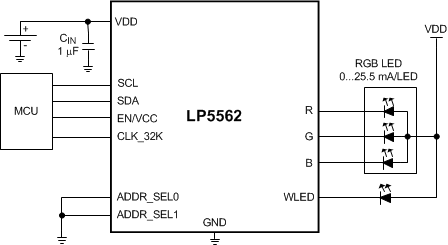
The LP5562 is a four-channel LED driver designed to produce variety of lighting effects. The device has a program memory for creating variety of lighting sequences. When the program memory has been loaded, the LP5562 can operate independently without processor control.
The LP5562 is able to automatically enter power save mode, when LED outputs are not active and thus lowering current consumption.
Four independent LED channels have accurate programmable current sinks, from 0 mA to 25.5 mA with 100-μA steps and flexible PWM control. Each channel can be configured into each of the three program execution engines. Program execution engines have program memory for creating desired lighting sequences with PWM control.
The LP5562 has four pin-selectable I2C addresses. This allows connecting up to four parallel devices in one I2C bus. The device requires only one small, low-cost ceramic capacitor.
Device Information(1)
| PART NUMBER | PACKAGE | BODY SIZE (MAX) |
|---|---|---|
| LP5562 | DSBGA (12) | 1.648 mm × 1.248 mm |
- For all available packages, see the orderable addendum at the end of the data sheet.
Typical Application Diagram
4 Revision History
Changes from A Revision (September 2015) to B Revision
- Changed title for SEO/keyword improvement Go
- Changed RθJA from "68°C/W" to "85.9°C/W"; added additional required thermal information Go
Changes from * Revision (April 2013) to A Revision
- Added Pin Configuration and Functions section, ESD Ratings table, Feature Description section, Device Functional Modes, Application and Implementation section, Power Supply Recommendations section, Layout section, Device and Documentation Support section, and Mechanical, Packaging, and Orderable Information section Go
5 Pin Configuration and Functions
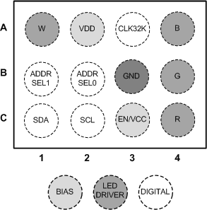
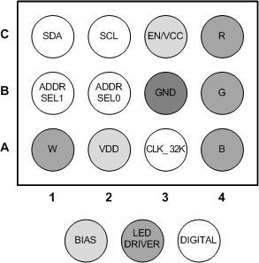
Pin Functions
| PIN | TYPE(1) | DESCRIPTION | |
|---|---|---|---|
| NUMBER | NAME | ||
| A1 | W | A | LED driver current sink terminal |
| A2 | VDD | P | Power supply |
| A3 | CLK_32K | I | External 32-kHz clock input |
| A4 | B | A | LED driver current sink terminal |
| B1 | ADDR_SEL1 | I | I2C address selection pin |
| B2 | ADDR_SEL0 | I | I2C address selection pin |
| B3 | GND | G | Ground |
| B4 | G | A | LED driver current sink terminal |
| C1 | SDA | I/O | I2C serial interface data input/output |
| C2 | SCL | I | I2C serial interface clock |
| C3 | EN/VCC | P | Enable/Logic power supply |
| C4 | R | A | LED driver current sink terminal |
6 Specifications
6.1 Absolute Maximum Ratings
over operating free-air temperature range (unless otherwise noted)(1)| MIN | MAX | UNIT | ||
|---|---|---|---|---|
| V (VDD, VEN/VCC, R, G, B, W) | −0.3 | 6 | V | |
| Voltage on pins | −0.3 | VDD + 0.3 with 6 V maximum | V | |
| Continuous power dissipation(2) | Internally limited | |||
| Junction temperature, TJ-MAX | 125 | °C | ||
| Maximum lead temperature (soldering) | See(3) | |||
| Storage temperature, Tstg | −65 | 150 | °C | |
6.2 ESD Ratings
| VALUE | UNIT | |||
|---|---|---|---|---|
| V(ESD) | Electrostatic discharge | Human-body model (HBM), per ANSI/ESDA/JEDEC JS-001(1) | ±1000 | V |
| Charged-device model (CDM), per JEDEC specification JESD22-C101(2) | ±250 | |||
6.3 Recommended Operating Conditions
over operating free-air temperature range (unless otherwise noted)| MIN | NOM | MAX | UNIT | ||
|---|---|---|---|---|---|
| VDD | 2.7 | 5.5 | V | ||
| VEN/VCC | 1.65 | VDD | V | ||
| Junction temperature, TJ | −40 | 125 | °C | ||
| Ambient temperature, TA(1) | −40 | 85 | °C | ||
(TJ-MAX-OP = 125°C), the maximum power dissipation of the device in the application (PD-MAX), and the junction-to ambient thermal resistance of the part/package in the application (RθJA), as given by the equation: TA-MAX = TJ-MAX-OP – (RθJA × PD-MAX).
6.4 Thermal Information
| THERMAL METRIC(1) | LP5562 | UNIT | |
|---|---|---|---|
| YQE (DSBGA) | |||
| 12 PINS | |||
| RθJA | Junction-to-ambient thermal resistance | 85.9 | °C/W |
| RθJC(top) | Junction-to-case (top) thermal resistance | 1.0 | °C/W |
| RθJB | Junction-to-board thermal resistance | 15.3 | °C/W |
| ψJT | Junction-to-top characterization parameter | 0.6 | °C/W |
| ψJB | Junction-to-board characterization parameter | 15.4 | °C/W |
6.5 Electrical Characteristics
Unless otherwise specified: limits for typical values are for TA = 25°C and minimum and maximum limits apply over the operating ambient temperature range (−40°C < TA < +85°C); VIN = 3.6V, VEN/VCC = 1.8 V.(1)(2)(3)| PARAMETER | TEST CONDITIONS | MIN | TYP | MAX | UNIT | |
|---|---|---|---|---|---|---|
| CURRENT CONSUMPTION AND OSCILLATOR ELECTRICAL CHARACTERISTICS | ||||||
| IVDD | Standby supply current | EN = 0 (pin), CHIP_EN = 0 (bit), external 32 kHz clock running or not running | 0.2 | 2 | µA | |
| EN = 1 (pin), CHIP_EN = 0 (bit), external 32 kHz clock not running |
2 | µA | ||||
| EN = 1 (pin), CHIP_EN = 0 (bit) External 32-kHz clock running |
2.4 | µA | ||||
| Normal mode supply current | LED drivers disabled | 0.25 | mA | |||
| LED drivers enabled | 1 | mA | ||||
| Powersave mode supply current | External 32-kHz clock running | 10 | µA | |||
| Internal oscillator running | 0.25 | mA | ||||
| ƒOSC | Internal oscillator frequency accuracy | TA = 25°C | –4% | 4% | ||
| –7% | 7% | |||||
| LED DRIVER ELECTRICAL CHARACTERISTICS (R, G, B, W OUTPUTS) | ||||||
| ILEAKAGE | R, G, B, W pin leakage current | TA = 25°C | 0.1 | 1 | µA | |
| IMAX | Maximum source current | Outputs R, G, B, W | 25.5 | mA | ||
| IOUT | Accuracy of output current(4) | Output current set to 17.5 mA, VDD = 3.6 V TA = 25°C |
–4% | 4% | ||
| Output current set to 17.5 mA, VDD = 3.6 V | –5% | 5% | ||||
| IMATCH | Matching(4) | Output current set to 17.5 mA, VDD = 3.6V | 1% | 2% | ||
| ƒLED | LED PWM switching frequency | PWM_HF = 1 | 558 | Hz | ||
| PWM_HF = 0 | 256 | |||||
| VSAT | Saturation voltage(5) | Output current set to 17.5 mA TA = 25°C |
60 | 100 | mV | |
6.6 Logic Interface Characteristics
Unless otherwise specified: limits for typical values are for TA = 25°C and minimum and maximum limits apply over the operating ambient temperature range (−40°C < TA < +85°C); VEN = 1.65 V.| PARAMETER | TEST CONDITIONS | MIN | TYP | MAX | UNIT | |
|---|---|---|---|---|---|---|
| LOGIC INPUT EN | ||||||
| VIL | Input low level | 0.5 | V | |||
| VIH | Input high level | 1.2 | V | |||
| II | Logic input current | –1 | 1 | µA | ||
| tDELAY | Input delay(1) | 2 | µs | |||
| LOGIC INPUT SCL, SDA, CLK_32K, ADDR_SEL0, ADDR_SEL1, VEN = 1.8 V | ||||||
| VIL | Input low level | 0.2 × VEN | V | |||
| VIH | Input high level | 0.8 × VEN | V | |||
| II | Input current | –1 | 1 | µA | ||
| ƒCLK_32K | Clock frequency | 32 | kHz | |||
| ƒSCL | Clock frequency | 400 | kHz | |||
| LOGIC OUTPUT SDA | ||||||
| VOL | Output low level | IOUT = 3 mA (pullup current) | 0.3 | 0.5 | V | |
| IL | Output leakage current | 1 | µA | |||
6.7 Recommended External Clock Source Conditions
over operating free-air temperature range (unless otherwise noted)(1)(2)| PARAMETER | TEST CONDITIONS | MIN | TYP | MAX | UNIT | |
|---|---|---|---|---|---|---|
| LOGIC INPUT CLK_32K | ||||||
| ƒCLK_32K | Clock frequency | 32.7 | kHz | |||
| tCLKH | High time | 6 | µs | |||
| tCLKL | Low time | 6 | µs | |||
| tr | Clock rise time | 10% to 90% | 2 | µs | ||
| tf | Clock fall time | 90% to 10% | 2 | µs | ||
6.8 I2C Timing Requirements (SDA, SCL)
See(1)| MIN | MAX | UNIT | ||
|---|---|---|---|---|
| ƒSCL | Clock frequency | 400 | kHz | |
| 1 | Hold time (repeated) START condition | 0.6 | µs | |
| 2 | Clock low time | 1.3 | µs | |
| 3 | Clock high time | 600 | ns | |
| 4 | Setup time for a repeated START condition | 600 | ns | |
| 5 | Data hold time | 50 | ns | |
| 6 | Data setup time | 100 | ns | |
| 7 | Rise time of SDA and SCL | 20 + 0.1Cb | 300 | ns |
| 8 | Fall time of SDA and SCL | 15 + 0.1Cb | 300 | ns |
| 9 | Set-up time for STOP condition | 600 | ns | |
| 10 | Bus-free time between a STOP and a START condition | 1.3 | µs | |
| Cb | Capacitive load for each bus line | 10 | 200 | pF |
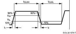 Figure 1. External Clock Timing
 Figure 2. I2C Timing Parameters
6.9 Typical Characteristics: Current Consumption
Unless otherwise specified: VDD = 3.6 V, VEN = 3.3 V. Here are presented input current consumption measurements. Current consumption is measured during a LED blink program execution. Program code sets every LED output to full PWM value for 2 seconds and then PWM is set to 0 for 2 seconds. This is looped endlessly. 750 measurements are taken during one measurement cycle.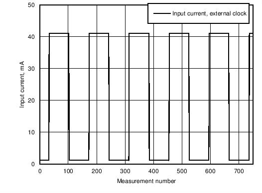 Figure 3. Input Current Consumption in Normal Mode With External Clock Running. 4 LEDs (RGBW) Set as Load. Every LED Driver Current Value Is Set to 10 mA.
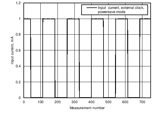 Figure 5. Input Current Consumption in Power Save Mode With External Clock Running, no LEDs as Load. All 4 LED Drivers are Enabled During Program Execution.
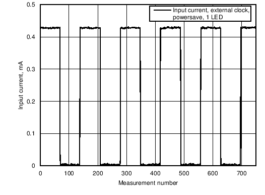 Figure 7. Input Current Consumption in Power Save Mode With External Clock Running, no LEDs as Load. Only 1 LED Driver is Enabled During Program Execution.
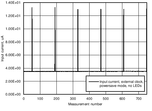 Figure 9. Input Current Consumption in Power Save Mode With External Clock Running, no LEDs as Load and no LED Drivers are Enabled During Program Execution.
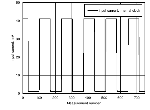 Figure 4. Input Current Consumption in Normal Mode With Internal Clock Running. 4 LEDs (RGBW) set as Load. Every LED Driver Current Value is Set to 10 mA .
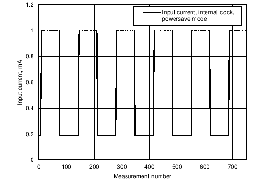 Figure 6. Input Current Consumption in Power Save Mode With Internal Clock Running, no LEDs as Load. All 4 LED Drivers are Enabled During Program Execution.
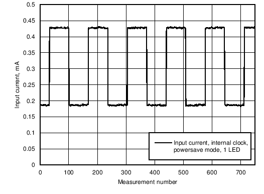 Figure 8. Input Current Consumption in Power Save Mode With Internal Clock Running, no LEDs as Load. Only 1 LED Driver is Enabled During Program Execution.
6.10 Typical Characteristics: LED Output
LED driver typical performance images.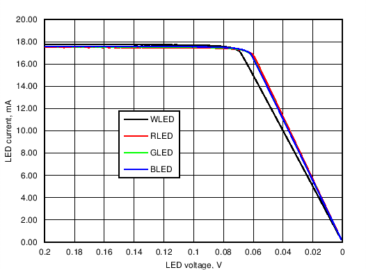 Figure 10. Every LED Driver Saturation Voltage, Current Setting 17.5 mA
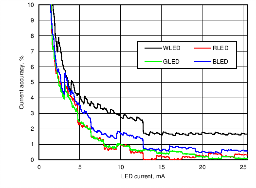 Figure 12. LED Driver Current Accuracy With Different Current Setting
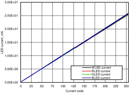 Figure 11. LED Driver Currents Compared to Current Setting Code
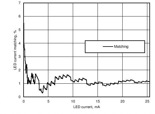 Figure 13. LED Driver Current Matching Between all LED Drivers With Different Current Setting