• Menu
  • Product
  • Email
  • PDF
  • Order now
  • DP83TD510E-EVM User’s Guide

    • SNLU271B March   2020  – June 2022 DP83TD510E


  • CONTENTS
  • SEARCH
  • DP83TD510E-EVM User’s Guide
  1.   DP83TD510E-EVM User’s Guide
  2.   Trademarks
  3. 1Definitions
  4. 2Introduction
    1. 2.1 Key Features
    2. 2.2 Block Diagram
    3. 2.3 Board Setup Out of Box
  5. 3Board Setup Details
    1. 3.1 Power Supply Selection
      1. 3.1.1 Onboard Power Supply Operation
      2. 3.1.2 External Power Supply Operation
      3. 3.1.3 USB Power Supply Option
    2. 3.2 Clock Selection – DP83TD510E
      1. 3.2.1 50 MHz Reference Clock for DP83TD510E in RMII Slave Mode
      2. 3.2.2 Enable External Clock on DP83TD510E Board
      3. 3.2.3 Enable On-Board 25 MHz Crystal for DP83RD510E Board
      4. 3.2.4 Enable On-Board 25 MHz Crystal for DP83822 Board
      5. 3.2.5 50 MHz Reference Clock for DP83822 Board in RMII Slave Mode
    3. 3.3 SMI Connection
    4. 3.4 Cable Assembly
    5. 3.5 LED Indication
    6. 3.6 Serial Management Interface
    7. 3.7 Configuration Options
      1. 3.7.1 Bootstrap Options
  6. 4Software
    1. 4.1 MSP430 Driver
    2. 4.2 USB-2-MDIO Software
  7. 5USB to MDIO procedure
  8. 6Schematics
    1. 6.1 Main Power Schematic
    2. 6.2 Main Block Schematic
    3. 6.3 Interface Schematic
    4. 6.4 Analog Front End Schematic
    5. 6.5 COMs Schematic
    6. 6.6 Header Board
    7. 6.7 Hardware Schematic
  9. 7Layout
    1. 7.1  Top Overlay
    2. 7.2  Top Layer Mask
    3. 7.3  Top Layer
    4. 7.4  Ground Layer 1
    5. 7.5  Signal Layer
    6. 7.6  Power Layer
    7. 7.7  Ground Layer 2
    8. 7.8  Bottom Layer
    9. 7.9  Bottom Layer Mask
    10. 7.10 Bottom Overlay
    11. 7.11 Board Assembly
  10. 8Bill of Materials
  11. 9Revision History
  12. IMPORTANT NOTICE
search No matches found.
  • Full reading width
    • Full reading width
    • Comfortable reading width
    • Expanded reading width
  • Card for each section
  • Card with all content


USER'S GUIDE

DP83TD510E-EVM User’s Guide

1 DP83TD510E-EVM User’s Guide

This User’s Guide discusses how to properly operate and configure the DP83TD510E-EVM. For best layout practices, schematic files, and Bill of Materials, see the associated support documents.
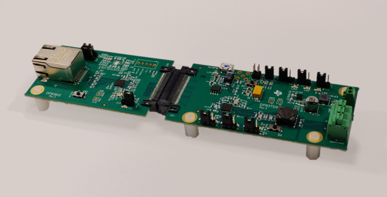
GUID-20200727-CA0I-L9D6-TNZJ-5FQKMGHHRDZS-low.pngFigure 1-1 DP83TD510E-EVM Consists of Two PCB's: The DP83TD510E Single-Pair-Ethernet Board and The DP83822I Media-Converter Board

Trademarks

All trademarks are the property of their respective owners.

1 Definitions

Table 1-1 Terminology
ACRONYMDEFINITION
PHYPhysical Layer Transceiver
MACMedia Access Controller
SMISerial Management Interface
MDIOManagement Data I/O
MDCManagement Data Clock
RGMIIReduced Gigabit Media Independent Interface
SFDStart-of-Frame Detection
VDDAAnalog Core Supply Rail
VDDIODigital Supply Rail
PDPulldown
PUPullup
MCMicrocontroller

AFE

Analog Front End

2 Introduction

The DP83TD510E-EVM supports 10-Mbps speed and is IEEE 802.3cg compliant. A DP83822I media converter board is provided for 10BASE-TX Standard Ethernet support and enables bit-error rate testing, interoperability testing, and PMA compliance testing. The EVM also provides on-board tools to configure PHY register using a USB-MDIO graphical user interface tool. The EVM can be powered by a Wide-Vin 5V-36V power supply or through a microUSB cable. Both the DP83TD510E and DP83822I can be set to RMII Master or Slave through an on-board 25-MHz crystal oscillator or the other's RMII 50-MHz clock, respectively.


Texas Instruments

© Copyright 1995-2025 Texas Instruments Incorporated. All rights reserved.
Submit documentation feedback | IMPORTANT NOTICE | Trademarks | Privacy policy | Cookie policy | Terms of use | Terms of sale