-
LMK04208 Low-Noise Clock Jitter Cleaner with Dual Loop PLLs
- 1 Features
- 2 Applications
- 3 Description
- 4 Revision History
- 5 Pin Configuration and Functions
- 6 Specifications
- 7 Parameter Measurement Information
-
8 Detailed Description
- 8.1
Overview
- 8.1.1 System Architecture
- 8.1.2 PLL1 Redundant Reference Inputs (CLKin0/CLKin0* and CLKin1/CLKin1*)
- 8.1.3 PLL1 Tunable Crystal Support
- 8.1.4 VCXO/Crystal Buffered Output
- 8.1.5 Frequency Holdover
- 8.1.6 Integrated Loop Filter Poles
- 8.1.7 Internal VCO
- 8.1.8 External VCO Mode
- 8.1.9 Clock Distribution
- 8.1.10 0-Delay
- 8.1.11 Default Startup Clocks
- 8.1.12 Status Pins
- 8.1.13 Register Readback
- 8.2 Functional Block Diagram
- 8.3
Feature Description
- 8.3.1 Inputs / Outputs
- 8.3.2 Input Clock Switching
- 8.3.3 Holdover Mode
- 8.3.4 PLLs
- 8.3.5 Status Pins
- 8.3.6 VCO
- 8.3.7 Clock Distribution
- 8.3.8 0-Delay Mode
- 8.4 Device Functional Modes
- 8.5 Programming
- 8.6
Register Maps
- 8.6.1 Register Map and Readback Register Map
- 8.6.2 Default Device Register Settings After Power On Reset
- 8.6.3
Register Descriptions
- 8.6.3.1
Registers R0 to R5
- 8.6.3.1.1 CLKoutX_PD, Powerdown CLKoutX Output Path
- 8.6.3.1.2 CLKoutX_OSCin_Sel, Clock Group Source
- 8.6.3.1.3 CLKoutX_ADLY_SEL, Select Analog Delay
- 8.6.3.1.4 CLKoutX_DDLY, Clock Channel Digital Delay
- 8.6.3.1.5 Reset
- 8.6.3.1.6 POWERDOWN
- 8.6.3.1.7 CLKoutX_HS, Digital Delay Half Shift
- 8.6.3.1.8 CLKoutX_DIV, Clock Output Divide
- 8.6.3.2 Registers R6 to R8
- 8.6.3.3 Register R10
- 8.6.3.4 Register R11
- 8.6.3.5 Register R12
- 8.6.3.6 Register R13
- 8.6.3.7 Register 14
- 8.6.3.8 Register 15
- 8.6.3.9 Register 16
- 8.6.3.10 Register 23
- 8.6.3.11
Register 24
- 8.6.3.11.1 PLL2_C4_LF, PLL2 Integrated Loop Filter Component
- 8.6.3.11.2 PLL2_C3_LF, PLL2 Integrated Loop Filter Component
- 8.6.3.11.3 PLL2_R4_LF, PLL2 Integrated Loop Filter Component
- 8.6.3.11.4 PLL2_R3_LF, PLL2 Integrated Loop Filter Component
- 8.6.3.11.5 PLL1_N_DLY
- 8.6.3.11.6 PLL1_R_DLY
- 8.6.3.11.7 PLL1_WND_SIZE
- 8.6.3.12 Register 25
- 8.6.3.13 Register 26
- 8.6.3.14 Register 27
- 8.6.3.15 Register 28
- 8.6.3.16 Register 29
- 8.6.3.17 Register 30
- 8.6.3.18 Register 31
- 8.6.3.1
Registers R0 to R5
- 8.1
Overview
-
9 Application and Implementation
- 9.1
Application Information
- 9.1.1 Loop Filter
- 9.1.2 Driving CLKin and OSCin Inputs
- 9.1.3 Termination and Use of Clock Output (Drivers)
- 9.1.4 Frequency Planning with the LMK04208
- 9.1.5 PLL Programming
- 9.1.6 Digital Lock Detect Frequency Accuracy
- 9.1.7 Calculating Dynamic Digital Delay Values for Any Divide
- 9.1.8 Optional Crystal Oscillator Implementation (OSCin/OSCin*)
- 9.2 Typical Applications
- 9.3 System Examples
- 9.4 Do's and Don'ts
- 9.1
Application Information
- 10Power Supply Recommendations
- 11Layout
- 12Device and Documentation Support
- 13Mechanical, Packaging, and Orderable Information
- IMPORTANT NOTICE
LMK04208 Low-Noise Clock Jitter Cleaner with Dual Loop PLLs
1 Features
- Ultra-Low RMS Jitter Performance
- 111 fs, RMS Jitter (12 kHz to 20 MHz)
- 123 fs, RMS Jitter (100 Hz to 20 MHz)
- Dual Loop PLLatinum™ PLL Architecture
- PLL1
- Integrated Low-Noise Crystal Oscillator Circuit
- Holdover Mode when Input Clocks are Lost
- Automatic or Manual Triggering/Recovery
- PLL2
- Normalized PLL Noise Floor of –227 dBc/Hz
- Phase Detector Rate of Up to 155 MHz
- OSCin Frequency-Doubler
- Integrated Low-Noise VCO or External VCO Mode
- Two Redundant Input Clocks with LOS
- Automatic and Manual Switch-Over Modes
- 50 % Duty Cycle Output Divides, 1 to 1045 (Even and Odd)
- 6 LVPECL, LVDS, or LVCMOS Programmable Outputs
- Digital Delay: Fixed or Dynamically Adjustable
- 25 ps Step Analog Delay Control
- 7 Differential Outputs, Up to 14 Single-Ended
- Up to 6 VCXO/Crystal Buffered Outputs
- Clock Rates of Up to 1536 MHz
- 0-Delay Mode
- Three Default Clock Outputs at Power Up
- Multi-Mode: Dual PLL, Single PLL, and Clock Distribution
- Industrial Temperature Range: –40°C to +85°C
- 3.15-V to 3.45-V Operation
- 64-Pin WQFN Package (9.0 × 9.0 × 0.8 mm)
2 Applications
- Data Converter Clocking
- Wireless Infrastructure
- Networking, SONET/SDH, DSLAM
- Medical, Video, Military, Aerospace
- Test and Measurement
3 Description
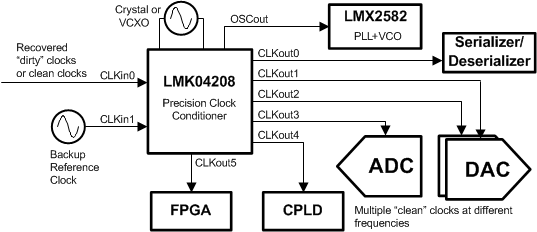
The LMK04208 is a high performance clock conditioner with superior clock jitter cleaning, generation, and distribution with advanced features to meet next generation system requirements. The dual loop PLLatinum™ architecture is capable of 111 fs, RMS jitter (12 kHz to 20 MHz) using a low-noise VCXO module or sub-200 fs rms jitter (12 kHz to 20 MHz) using a low cost external crystal and varactor diode.
The dual loop architecture consists of two high-performance phase-locked loops (PLL), a low-noise crystal oscillator circuit, and a high-performance voltage controlled oscillator (VCO). The first PLL (PLL1) provides low-noise jitter cleaner functionality while the second PLL (PLL2) performs the clock generation. PLL1 can be configured to either work with an external VCXO module or the integrated crystal oscillator with an external tunable crystal and varactor diode. When paired with a very narrow loop bandwidth, PLL1 uses the superior close-in phase noise (offsets below 50 kHz) of the VCXO module or the tunable crystal to clean the input clock. The output of PLL1 is used as the clean input reference to PLL2 where it locks the integrated VCO. The loop bandwidth of PLL2 can be optimized to clean the far-out phase noise (offsets above 50 kHz) where the integrated VCO outperforms the VCXO module or tunable crystal used in PLL1.
Device Information(1)
| PART NUMBER | VCO FREQUENCY | CLOCK INPUTS |
|---|---|---|
| LMK04208 | 2750 to 3072 MHz | 2 |
- For all available packages, see the orderable addendum at the end of the data sheet.
Simplified Schematic
4 Revision History
| DATE | REVISION | NOTES |
|---|---|---|
| September 2016 | * | Initial release. |
5 Pin Configuration and Functions
Pin Functions(1)
| PIN | I/O | TYPE | DESCRIPTION | |
|---|---|---|---|---|
| NO. | NAME | |||
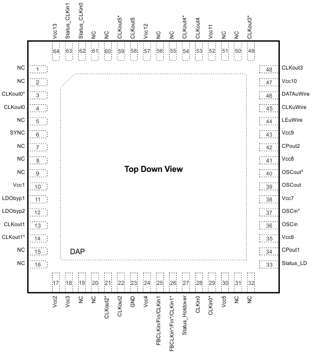
| 1, 2 | NC | – | – | No Connection. These pins must be left floating. |
| 3, 4 | CLKout0*, CLKout0 | O | Programmable | Clock output 0. |
| 5 | NC | – | – | No Connection. These pins must be left floating. |
| 6 | SYNC | I/O | Programmable | CLKout Synchronization input or programmable status pin. |
| 7, 8, 9 | NC | – | – | No Connection. These pins must be left floating. |
| 10 | Vcc1 | PWR | Power supply for VCO LDO. | |
| 11 | LDObyp1 | ANLG | LDO Bypass, bypassed to ground with 10-µF capacitor. | |
| 12 | LDObyp2 | ANLG | LDO Bypass, bypassed to ground with a 0.1-µF capacitor. | |
| 13, 14 | CLKout1, CLKout1* | O | Programmable | Clock output 1. |
| 15, 16 | NC | – | – | No Connection. These pins must be left floating. |
| 17 | Vcc2 | PWR | Power supply for clock output 1. | |
| 18 | Vcc3 | PWR | Power supply for clock output 2. | |
| 19, 20 | NC | – | – | No Connection. These pins must be left floating. |
| 21, 22 | CLKout2*, CLKout2 | O | Programmable | Clock output 2. |
| 23 | GND | PWR | Ground. | |
| 24 | Vcc4 | PWR | Power supply for digital. | |
| 25, 26 | CLKin1, CLKin1* | I | ANLG | Reference Clock Input Port 1 for PLL1. AC or DC Coupled. |
| FBCLKin, FBCLKin* | Feedback input for external clock feedback input (0-delay mode). AC or DC Coupled. | |||
| Fin/Fin* | External VCO input (External VCO mode). AC or DC Coupled. | |||
| 27 | Status_Holdover | I/O | Programmable | Programmable status pin, default readback output. Programmable to holdover mode indicator. Other options available by programming. |
| 28, 29 | CLKin0, CLKin0* | I | ANLG | Reference Clock Input Port 0 for PLL1. AC or DC Coupled. |
| 30 | Vcc5 | PWR | Power supply for clock inputs. | |
| 31, 32 | NC | – | – | No Connection. These pins must be left floating. |
| 33 | Status_LD | I/O | Programmable | Programmable status pin, default lock detect for PLL1 and PLL2. Other options available by programming. |
| 34 | CPout1 | O | ANLG | Charge pump 1 output. |
| 35 | Vcc6 | PWR | Power supply for PLL1, charge pump 1. | |
| 36, 37 | OSCin, OSCin* | I | ANLG | Feedback to PLL1, Reference input to PLL2. AC Coupled. |
| 38 | Vcc7 | PWR | Power supply for OSCin, OSCout, and PLL2 circuitry.(2) | |
| 39, 40 | OSCout, OSCout* | O | Programmable | Buffered output of OSCin port.(2) |
| 41 | Vcc8 | PWR | Power supply for PLL2, charge pump 2. | |
| 42 | CPout2 | O | ANLG | Charge pump 2 output. |
| 43 | Vcc9 | PWR | Power supply for PLL2. | |
| 44 | LEuWire | I | CMOS | MICROWIRE Latch Enable Input. |
| 45 | CLKuWire | I | CMOS | MICROWIRE Clock Input. |
| 46 | DATAuWire | I | CMOS | MICROWIRE Data Input. |
| 47 | Vcc10 | PWR | Power supply for clock output 3. | |
| 48, 49 | CLKout3, CLKout3* | O | Programmable | Clock output 3. |
| 50, 51 | NC | – | – | No Connection. These pins must be left floating. |
| 52 | Vcc11 | PWR | Power supply for clock output 4. | |
| 53, 54 | CLKout4, CLKout4* | O | Programmable | Clock output 4. |
| 55, 56 | NC | – | – | No Connection. These pins must be left floating. |
| 57 | Vcc12 | PWR | Power supply for clock output 5. | |
| 58, 59 | CLKout5, CLKout5* | O | Programmable | Clock output 5. |
| 60, 61 | NC | – | – | No Connection. These pins must be left floating. |
| 62 | Status_CLKin0 | I/O | Programmable | NC. Programmable status pin. Default is input for pin control of PLL1 reference clock selection. CLKin0 LOS status and other options available by programming. |
| 63 | Status_CLKin1 | I/O | Programmable | Programmable status pin. Default is input for pin control of PLL1 reference clock selection. CLKin1 LOS status and other options available by programming. |
| 64 | Vcc13 | PWR | Power supply for clock output 0. | |
| DAP | DAP | – | GND | DIE ATTACH PAD, connect to GND. |
6 Specifications
6.1 Absolute Maximum Ratings
over operating free-air temperature range (unless otherwise noted)(1)(3)(1)| MIN | MAX | UNIT | ||
|---|---|---|---|---|
| VCC | Supply voltage (2) | –0.3 | 3.6 | V |
| VIN | Input voltage | –0.3 | VCC + 0.3 | V |
| TL | Lead temperature (solder 4 seconds) | 260 | °C | |
| TJ | Junction temperature | 150 | °C | |
| IIN | Differential input current (CLKinX/X*, OSCin/OSCin*, FBCLKin/FBCLKin*, Fin/Fin*) |
± 5 | mA | |
| MSL | Moisture Sensitivity Level | 3 | ||
| Tstg | Storage temperature | -65 | 150 | °C |
6.2 ESD Ratings
| VALUE | UNIT | |||
|---|---|---|---|---|
| V(ESD) | Electrostatic discharge | Human-body model (HBM), per ANSI/ESDA/JEDEC JS-001(1) | ±2000 | V |
| Charged-device model (CDM), per JEDEC specification JESD22-C101(2) | ±750 | |||
6.3 Recommended Operating Conditions
| MIN | NOM | MAX | UNIT | |||
|---|---|---|---|---|---|---|
| TJ | Junction temperature | 125 | °C | |||
| TA | Ambient temperature | VCC = 3.3 V | –40 | 25 | 85 | °C |
| VCC | Supply voltage | 3.15 | 3.3 | 3.45 | V | |
6.4 Thermal Information
| THERMAL METRIC(1) | LMK04208 | UNIT | |
|---|---|---|---|
| NKD (WQFN) | |||
| 64 PINS | |||
| RθJA | Junction-to-ambient thermal resistance on 4-layer JEDEC PCB(2)(8) | 25.2 | °C/W |
| RθJC(top) | Junction-to-case (top) thermal resistance(3)(9) | 6.9 | °C/W |
| RθJB | Junction-to-board thermal resistance(4) | 4.0 | °C/W |
| ψJT | Junction-to-top characterization parameter(5) | 0.1 | °C/W |
| ψJB | Junction-to-board characterization parameter(6) | 4.0 | °C/W |
| RθJC(bot) | Junction-to-case (bottom) thermal resistance(7) | 0.8 | °C/W |
6.5 Electrical Characteristics
3.15 V ≤ VCC ≤ 3.45 V, –40 °C ≤ TA ≤ 85°C. Typical values represent most likely parametric norms at VCC = 3.3 V, TA = 25°C, at the Recommended Operating Conditions at the time of product characterization and are not specified.(4)| PARAMETER | TEST CONDITIONS | MIN | TYP | MAX | UNIT | |
|---|---|---|---|---|---|---|
| CURRENT CONSUMPTION | ||||||
| ICC_PD | Power down supply current | 1 | 3 | mA | ||
| ICC_CLKS | Supply current with all clocks (CLKoutX) and OSCout enabled as LVDS.(2) | All clock delays disabled, CLKoutX_DIV = 1045, EN_SYNC=0 PLL1 and PLL2 locked. |
445 | 535 | mA | |
| CLKin0/0* and CLKin1/1* INPUT CLOCK SPECIFICATIONS | ||||||
| fCLKin | Clock input frequency(3) | 0.001 | 500 | MHz | ||
| SLEWCLKin(4) | Clock input slew rate(17) | 20% to 80% | 0.15 | 0.5 | V/ns | |
| VIDCLKin | Clock input Differential input voltage (see (1) and Figure 8) |
AC coupled CLKinX_BUF_TYPE = 0 (Bipolar) |
0.25 | 1.55 | |V| | |
| VSSCLKin | 0.5 | 3.1 | Vpp | |||
| VIDCLKin | AC coupled CLKinX_BUF_TYPE = 1 (MOS) |
0.25 | 1.55 | |V| | ||
| VSSCLKin | 0.5 | 3.1 | Vpp | |||
| VCLKin | Clock input Single-ended input voltage(17) |
AC coupled to CLKinX; CLKinX* AC coupled to Ground CLKinX_BUF_TYPE = 0 (Bipolar) |
0.25 | 2.4 | Vpp | |
| AC coupled to CLKinX; CLKinX* AC coupled to Ground CLKinX_BUF_TYPE = 1 (MOS) |
0.25 | 2.4 | Vpp | |||
| VCLKin0-offset | DC offset voltage between CLKin0/CLKin0* CLKin0* - CLKin0 |
Each pin AC coupled CLKin0_BUF_TYPE = 0 (Bipolar) |
20 | mV | ||
| VCLKin1-offset | DC offset voltage between CLKin1/CLKin1* CLKin1* - CLKin1 |
0 | mV | |||
| VCLKinX-offset | DC offset voltage between CLKinX/CLKinX* CLKinX* - CLKinX |
Each pin AC coupled CLKinX_BUF_TYPE = 1 (MOS) |
55 | mV | ||
| VCLKin- VIH | High input voltage | DC coupled to CLKinX; CLKinX* AC coupled to Ground CLKinX_BUF_TYPE = 1 (MOS) |
2.0 | VCC | V | |
| VCLKin- VIL | Low input voltage | 0.0 | 0.4 | V | ||
| FBCLKin/FBCLKin* and Fin/Fin* INPUT SPECIFICATIONS | ||||||
| fFBCLKin | Clock input frequency(17) | AC coupled (CLKinX_BUF_TYPE = 0) MODE = 2 or 8; FEEDBACK_MUX = 6 |
0.001 | 1000 | MHz | |
| fFin | Clock input frequency(17) | AC coupled (CLKinX_BUF_TYPE = 0) MODE = 3 or 11 |
0.001 | 3100 | MHz | |
| VFBCLKin/Fin | Single Ended Clock input voltage(17) |
AC coupled; (CLKinX_BUF_TYPE = 0) |
0.25 | 2.0 | Vpp | |
| SLEWFBCLKin/Fin | Slew rate on CLKin(17)(4) | AC coupled; 20% to 80%; (CLKinX_BUF_TYPE = 0) |
0.15 | 0.5 | V/ns | |
| PLL1 SPECIFICATIONS | ||||||
| fPD1 | PLL1 phase detector frequency | 40 | MHz | |||
| ICPout1SOURCE | PLL1 charge Pump source current(5) |
VCPout1 = VCC/2, PLL1_CP_GAIN = 0 | 100 | µA | ||
| VCPout1 = VCC/2, PLL1_CP_GAIN = 1 | 200 | |||||
| VCPout1 = VCC/2, PLL1_CP_GAIN = 2 | 400 | |||||
| VCPout1 = VCC/2, PLL1_CP_GAIN = 3 | 1600 | |||||
| ICPout1SINK | PLL1 charge Pump sink current(5) |
VCPout1=VCC/2, PLL1_CP_GAIN = 0 | –100 | µA | ||
| VCPout1=VCC/2, PLL1_CP_GAIN = 1 | –200 | |||||
| VCPout1=VCC/2, PLL1_CP_GAIN = 2 | –400 | |||||
| VCPout1=VCC/2, PLL1_CP_GAIN = 3 | –1600 | |||||
| ICPout1%MIS | Charge pump Sink/source mismatch |
VCPout1 = VCC/2, T = 25 °C | 3% | 10% | ||
| ICPout1VTUNE | Magnitude of charge pump current variation vs. charge pump voltage | 0.5 V < VCPout1 < VCC - 0.5 V TA = 25 °C |
4% | |||
| ICPout1%TEMP | Charge pump current vs. temperature variation |
4% | ||||
| ICPout1 TRI | Charge Pump TRI-STATE leakage current | 0.5 V < VCPout < VCC - 0.5 V | 5 | nA | ||
| PN10kHz | PLL 1/f noise at 10 kHz offset.(9) Normalized to 1 GHz Output Frequency | PLL1_CP_GAIN = 400 µA | –117 | dBc/Hz | ||
| PLL1_CP_GAIN = 1600 µA | –118 | |||||
| PN1Hz | Normalized phase noise contribution(10) | PLL1_CP_GAIN = 400 µA | –221.5 | dBc/Hz | ||
| PLL1_CP_GAIN = 1600 µA | –223 | |||||
| PLL2 REFERENCE INPUT (OSCin) SPECIFICATIONS | ||||||
| fOSCin | PLL2 reference input(6) | 500 | MHz | |||
| SLEWOSCin | PLL2 reference clock minimum slew rate on OSCin(17) | 20% to 80% | 0.15 | 0.5 | V/ns | |
| VOSCin | Input voltage for OSCin or OSCin*(17) | AC coupled; Single-ended (Unused pin AC coupled to GND) | 0.2 | 2.4 | Vpp | |
| VIDOSCin | Differential voltage swing (see Figure 8) | AC coupled | 0.2 | 1.55 | |V| | |
| VSSOSCin | 0.4 | 3.1 | Vpp | |||
| VOSCin-offset | DC offset voltage between OSCin/OSCin* OSCinX* - OSCinX |
Each pin AC coupled | 20 | mV | ||
| fdoubler_max | Doubler input frequency(17) | EN_PLL2_REF_2X = 1;(7)
OSCin Duty Cycle 40% to 60% |
155 | MHz | ||
| CRYSTAL OSCILLATOR MODE SPECIFICATIONS | ||||||
| fXTAL | Crystal frequency range(17) | RESR < 40 Ω | 6 | 20.5 | MHz | |
| PXTAL | Crystal power dissipation(8) | Vectron VXB1 crystal, 20.48 MHz, RESR < 40 Ω XTAL_LVL = 0 |
100 | µW | ||
| CIN | Input capacitance of LMK04208 OSCin port |
-40 to +85 °C | 6 | pF | ||
| PLL2 PHASE DETECTOR and CHARGE PUMP SPECIFICATIONS | ||||||
| fPD2 | Phase detector frequency | 155 | MHz | |||
| ICPoutSOURCE | PLL2 charge pump source current(5) | VCPout2=VCC/2, PLL2_CP_GAIN = 0 | 100 | µA | ||
| VCPout2=VCC/2, PLL2_CP_GAIN = 1 | 400 | |||||
| VCPout2=VCC/2, PLL2_CP_GAIN = 2 | 1600 | |||||
| VCPout2=VCC/2, PLL2_CP_GAIN = 3 | 3200 | |||||
| ICPoutSINK | PLL2 charge pump sink current(5) | VCPout2=VCC/2, PLL2_CP_GAIN = 0 | –100 | µA | ||
| VCPout2=VCC/2, PLL2_CP_GAIN = 1 | –400 | |||||
| VCPout2=VCC/2, PLL2_CP_GAIN = 2 | –1600 | |||||
| VCPout2=VCC/2, PLL2_CP_GAIN = 3 | –3200 | |||||
| ICPout2%MIS | Charge pump sink/source mismatch | VCPout2=VCC/2, TA = 25 °C | 3% | 10% | ||
| ICPout2VTUNE | Magnitude of charge pump current vs. charge pump voltage variation | 0.5 V < VCPout2 < VCC - 0.5 V TA = 25 °C |
4% | |||
| ICPout2%TEMP | Charge pump current vs. Temperature variation |
4% | ||||
| ICPout2TRI | Charge pump leakage | 0.5 V < VCPout2 < VCC - 0.5 V | 10 | nA | ||
| PN10kHz | PLL 1/f Noise at 10 kHz offset(9)
Normalized to 1 GHz output frequency |
PLL2_CP_GAIN = 400 µA | –118 | dBc/Hz | ||
| PLL2_CP_GAIN = 3200 µA | –121 | |||||
| PN1Hz | Normalized Phase Noise Contribution(10) | PLL2_CP_GAIN = 400 µA | –222.5 | dBc/Hz | ||
| PLL2_CP_GAIN = 3200 µA | –227 | |||||
| INTERNAL VCO SPECIFICATIONS | ||||||
| fVCO | VCO tuning range | LMK04208 | 2750 | 3072 | MHz | |
| KVCO | Fine tuning sensitivity (The range displayed in the typical column indicates the lower sensitivity is typical at the lower end of the tuning range, and the higher tuning sensitivity is typical at the higher end of the tuning range). |
LMK04208 | 20 to 36 | MHz/V | ||
| |ΔTCL| | Allowable Temperature Drift for Continuous Lock(11) (17) | After programming R30 for lock, no changes to output configuration are permitted to ensure continuous lock | 125 | °C | ||
| CLKout CLOSED LOOP JITTER SPECIFICATIONS USING a COMMERCIAL QUALITY VCXO(14) | ||||||
| L(f)CLKout | LMK04208 fCLKout = 245.76 MHz SSB Phase noise Measured at clock outputs Value is average for all output types(12) |
Offset = 1 kHz | –122.5 | dBc/Hz | ||
| Offset = 10 kHz | –132.9 | |||||
| Offset = 100 kHz | –135.2 | |||||
| Offset = 800 kHz | –143.9 | |||||
| Offset = 10 MHz; LVDS | –156.0 | |||||
| Offset = 10 MHz; LVPECL 1600 mVpp | –157.5 | |||||
| Offset = 10 MHz; LVCMOS | –157.1 | |||||
| JCLKout
LVDS/LVPECL/LVCMOS |
LMK04208(12)
fCLKout = 245.76 MHz Integrated RMS jitter |
BW = 12 kHz to 20 MHz | 111 | fs, RMS | ||
| BW = 100 Hz to 20 MHz | 123 | |||||
| CLKout CLOSED LOOP JITTER SPECIFICATIONS USING THE INTEGRATED LOW NOISE CRYSTAL OSCILLATOR CIRCUIT (15) | ||||||
| LMK04208 fCLKout = 245.76 MHz Integrated RMS jitter |
BW = 12 kHz to 20 MHz XTAL_LVL = 3 |
192 | fs rms | |||
| BW = 100 Hz to 20 MHz XTAL_LVL = 3 |
450 | |||||
| DEFAULT POWER ON RESET CLOCK OUTPUT FREQUENCY | ||||||
| fCLKout-startup | Default output clock frequency at device power on(16) | CLKout4, LVDS, LMK04208 | 90 | 110 | 130 | MHz |
| CLOCK SKEW and DELAY | ||||||
| |TSKEW| | Maximum CLKoutX to CLKoutY(17)(13) | LVDS-to-LVDS, T = 25 °C, FCLK = 800 MHz, RL= 100 Ω AC coupled |
30 | ps | ||
| LVPECL-to-LVPECL, T = 25 °C, FCLK = 800 MHz, RL= 100 Ω emitter resistors = 240 Ω to GND AC coupled |
30 | |||||
| Maximum skew between any two LVCMOS outputs, same CLKout or different CLKout(17)(13) | RL = 50 Ω, CL = 5 pF, T = 25 °C, FCLK = 100 MHz. |
100 | ||||
| MixedTSKEW | LVDS or LVPECL to LVCMOS | Same device, T = 25 °C, 250 MHz |
750 | ps | ||
| td0-DELAY | CLKin to CLKoutX delay(13) | MODE = 2 PLL1_R_DLY = 0; PLL1_N_DLY = 0 |
1850 | ps | ||
| MODE = 2 PLL1_R_DLY = 0; PLL1_N_DLY = 0; VCO Frequency = 2949.12 MHz Analog delay select = 0; Feedback clock digital delay = 11; Feedback clock half step = 1; Output clock digital delay = 5; Output clock half step = 0; |
0 | |||||
| LVDS CLOCK OUTPUTS (CLKoutX), CLKoutX_TYPE = 1 | ||||||
| fCLKout | Maximum frequency(17)(18) | RL = 100 Ω | 1536 | MHz | ||
| VOD | Differential output voltage (see Figure 9) | T = 25 °C, DC measurement AC coupled to receiver input R = 100-Ω differential termination |
250 | 400 | 450 | |mV| |
| VSS | 500 | 800 | 900 | mVpp | ||
| ΔVOD | Change in magnitude of VOD for complementary output states | –50 | 50 | mV | ||
| VOS | Output offset voltage | 1.125 | 1.25 | 1.375 | V | |
| ΔVOS | Change in VOS for complementary output states | 35 | |mV| | |||
| TR / TF | Output rise time | 20% to 80%, RL = 100 Ω | 200 | ps | ||
| Output fall time | 80% to 20%, RL = 100 Ω | |||||
| ISA
ISB |
Output short circuit current single-ended |
Single-ended output shorted to GND T = 25 °C |
–24 | 24 | mA | |
| ISAB | Output short circuit current - differential | Complimentary outputs tied together | –12 | 12 | mA | |
| LVPECL CLOCK OUTPUTS (CLKoutX) | ||||||
| fCLKout | Maximum frequency(17)(18) | 1536 | MHz | |||
| TR / TF | 20% to 80% output rise | RL = 100 Ω, emitter resistors = 240 Ω to GND CLKoutX_TYPE = 4 or 5 (1600 or 2000 mVpp) |
150 | ps | ||
| 80% to 20% output fall time | ||||||
| 700-mVpp LVPECL CLOCK OUTPUTS (CLKoutX), CLKoutX_TYPE = 2 | ||||||
| VOH | Output high voltage | T = 25 °C, DC measurement Termination = 50 Ω to VCC - 1.4 V |
VCC – 1.03 | V | ||
| VOL | Output low voltage | VCC – 1.41 | V | |||
| VOD | Output voltage (see Figure 9) | 305 | 380 | 440 | |mV| | |
| VSS | 610 | 760 | 880 | mVpp | ||
| 1200-mVpp LVPECL CLOCK OUTPUTS (CLKoutX), CLKoutX_TYPE = 3 | ||||||
| VOH | Output high voltage | T = 25 °C, DC measurement Termination = 50 Ω to VCC - 1.7 V |
VCC – 1.07 | V | ||
| VOL | Output low voltage | VCC – 1.69 | V | |||
| VOD | Output voltage (see Figure 9) | 545 | 625 | 705 | |mV| | |
| VSS | 1090 | 1250 | 1410 | mVpp | ||
| 1600-mVpp LVPECL CLOCK OUTPUTS (CLKoutX), CLKoutX_TYPE = 4 | ||||||
| VOH | Output high voltage | T = 25 °C, DC Measurement Termination = 50 Ω to VCC - 2.0 V |
VCC – 1.10 | V | ||
| VOL | Output low voltage | VCC – 1.97 | V | |||
| VOD | Output voltage (see Figure 9) | 660 | 870 | 965 | |mV| | |
| VSS | 1320 | 1740 | 1930 | mVpp | ||
| 2000-mVpp LVPECL (2VPECL) CLOCK OUTPUTS (CLKoutX), CLKoutX_TYPE = 5 | ||||||
| VOH | Output high voltage | T = 25 °C, DC Measurement Termination = 50 Ω to VCC - 2.3 V |
VCC – 1.13 | V | ||
| VOL | Output low voltage | VCC – 2.20 | V | |||
| VOD | Output voltage Figure 9 | 800 | 1070 | 1200 | |mV| | |
| VSS | 1600 | 2140 | 2400 | mVpp | ||
| LVCMOS CLOCK OUTPUTS (CLKoutX) | ||||||
| fCLKout | Maximum frequency(17)(18) | 5 pF Load | 250 | MHz | ||
| VOH | Output high voltage | 1 mA Load | VCC – 0.1 | V | ||
| VOL | Output low voltage | 1 mA Load | 0.1 | V | ||
| IOH | Output high current (source) | VCC = 3.3 V, VO = 1.65 V | 28 | mA | ||
| IOL | Output low current (sink) | VCC = 3.3 V, VO = 1.65 V | 28 | mA | ||
| DUTYCLK | Output duty cycle(17) | VCC/2 to VCC/2, FCLK = 100 MHz T = 25 °C |
45% | 50% | 55% | |
| TR | Output rise time | 20% to 80%, RL = 50 Ω, CL = 5 pF |
400 | ps | ||
| TF | Output fall time | 80% to 20%, RL = 50 Ω, CL = 5 pF |
400 | ps | ||
| DIGITAL OUTPUTS (Status_CLKinX, Status_LD, Status_Holdover, SYNC) | ||||||
| VOH | High-level output voltage | IOH = -500 µA | VCC – 0.4 | V | ||
| VOL | Low-level output voltage | IOL = 500 µA | 0.4 | V | ||
| DIGITAL INPUTS (Status_CLKinX, SYNC) | ||||||
| VIH | High-level input voltage | 1.6 | VCC | V | ||
| VIL | Low-level input voltage | 0.4 | V | |||
| IIH | High-level input current VIH = VCC |
Status_CLKinX_TYPE = 0 (High Impedance) |
–5 | 5 | µA | |
| Status_CLKinX_TYPE = 1 (Pull-up) |
–5 | 5 | ||||
| Status_CLKinX_TYPE = 2 (Pull-down) |
10 | 80 | ||||
| IIL | Low-level input current VIL = 0 V |
Status_CLKinX_TYPE = 0 (High Impedance) |
–5 | 5 | µA | |
| Status_CLKinX_TYPE = 1 (Pull-up) |
–40 | -5 | ||||
| Status_CLKinX_TYPE = 2 (Pull-down) |
–5 | 5 | ||||
| DIGITAL INPUTS (CLKuWire, DATAuWire, LEuWire) | ||||||
| VIH | High-level input voltage | 1.6 | VCC | V | ||
| VIL | Low-level input voltage | 0.4 | V | |||
| IIH | High-level input current | VIH = VCC | 5 | 25 | µA | |
| IIL | Low-level input current | VIL = 0 | –5 | 5 | µA | |
6.6 Timing Requirements
See Programming for additional information| MIN | NOM | MAX | UNIT | |||
|---|---|---|---|---|---|---|
| TECS | LE to clock set up time | See Figure 1 through Figure 4 | 25 | ns | ||
| TDCS | Data to clock set up time | See Figure 1 | 25 | ns | ||
| TCDH | Clock to data hold time | See Figure 1 | 8 | ns | ||
| TCWH | Clock pulse width high | See Figure 1, Figure 2, and Figure 4 | 25 | ns | ||
| TCWL | Clock pulse width low | See Figure 1, Figure 2, and Figure 4 | 25 | ns | ||
| TCES | Clock to LE set up time | See Figure 1 through Figure 4 | 25 | ns | ||
| TEWH | LE pulse width | See Figure 1, Figure 2, and Figure 4 | 25 | ns | ||
| TCR | Falling clock to readback time | See Figure 4 | 25 | ns | ||
 Figure 1. MICROWIRE Input Timing Diagram
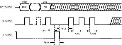 Figure 2. MICROWIRE Timing Diagram: Extra CLKuWire Pulses for R0 to R5
 Figure 3. MICROWIRE Timing Diagram: Extra CLKuWire Pulses for R0 to R5 with LEuWire Asserted
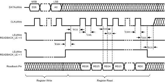 Figure 4. MICROWIRE Readback Timing Diagram
6.7 Typical Characteristics
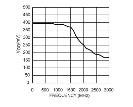
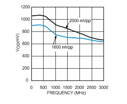
VOD vs Frequency
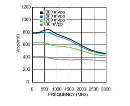
VOD vs Frequency
7 Parameter Measurement Information
7.1 Charge Pump Current Specification Definitions
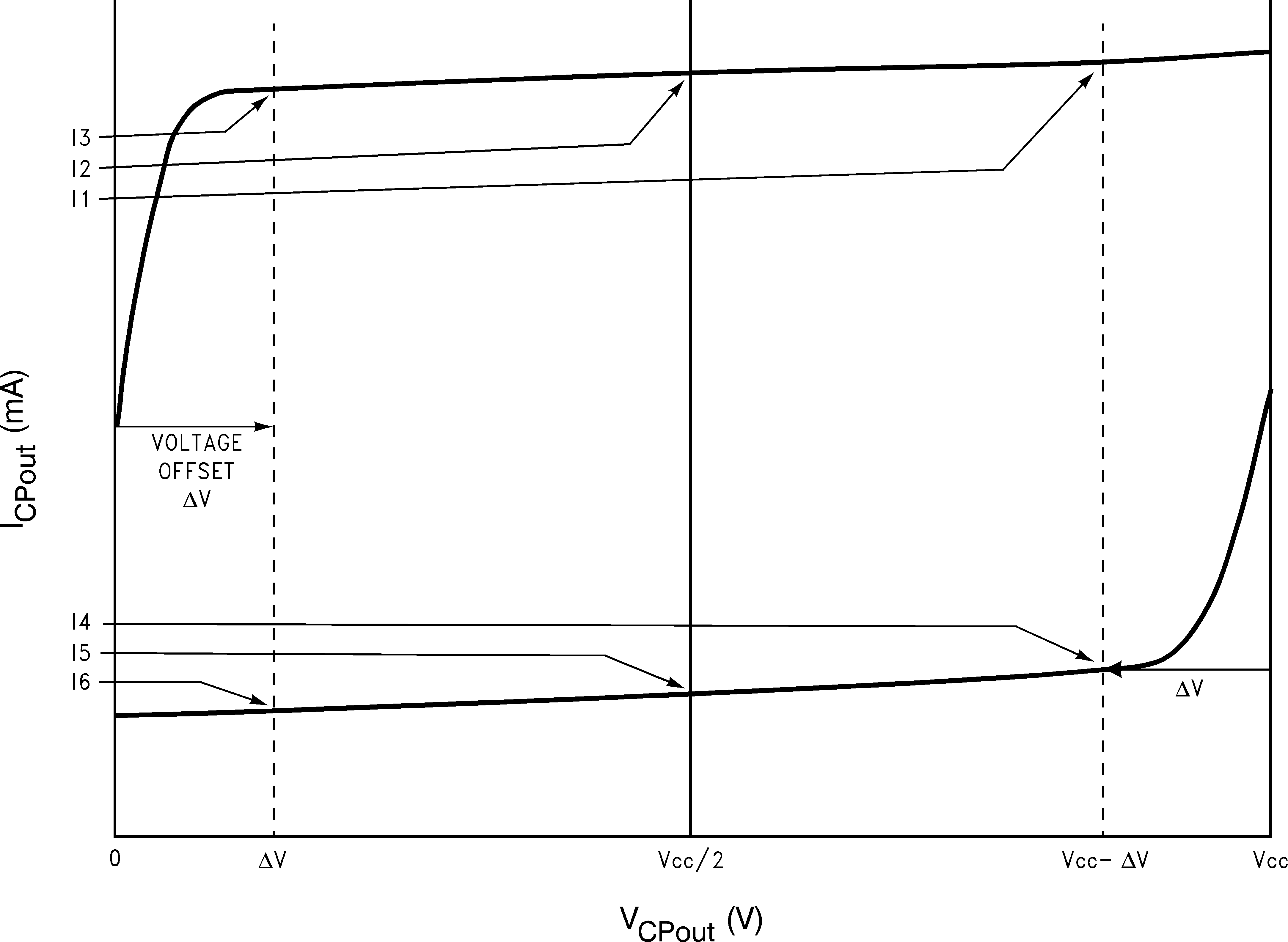
7.1.1 Charge Pump Output Current Magnitude Variation Vs. Charge Pump Output Voltage
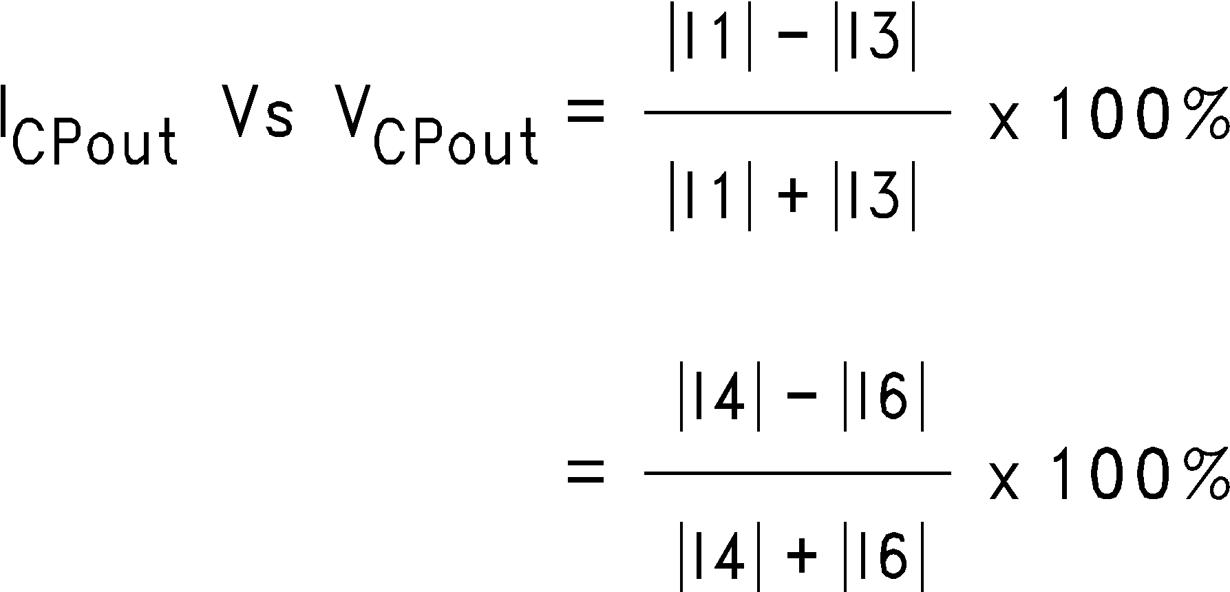
7.1.2 Charge Pump Sink Current Vs. Charge Pump Output Source Current Mismatch

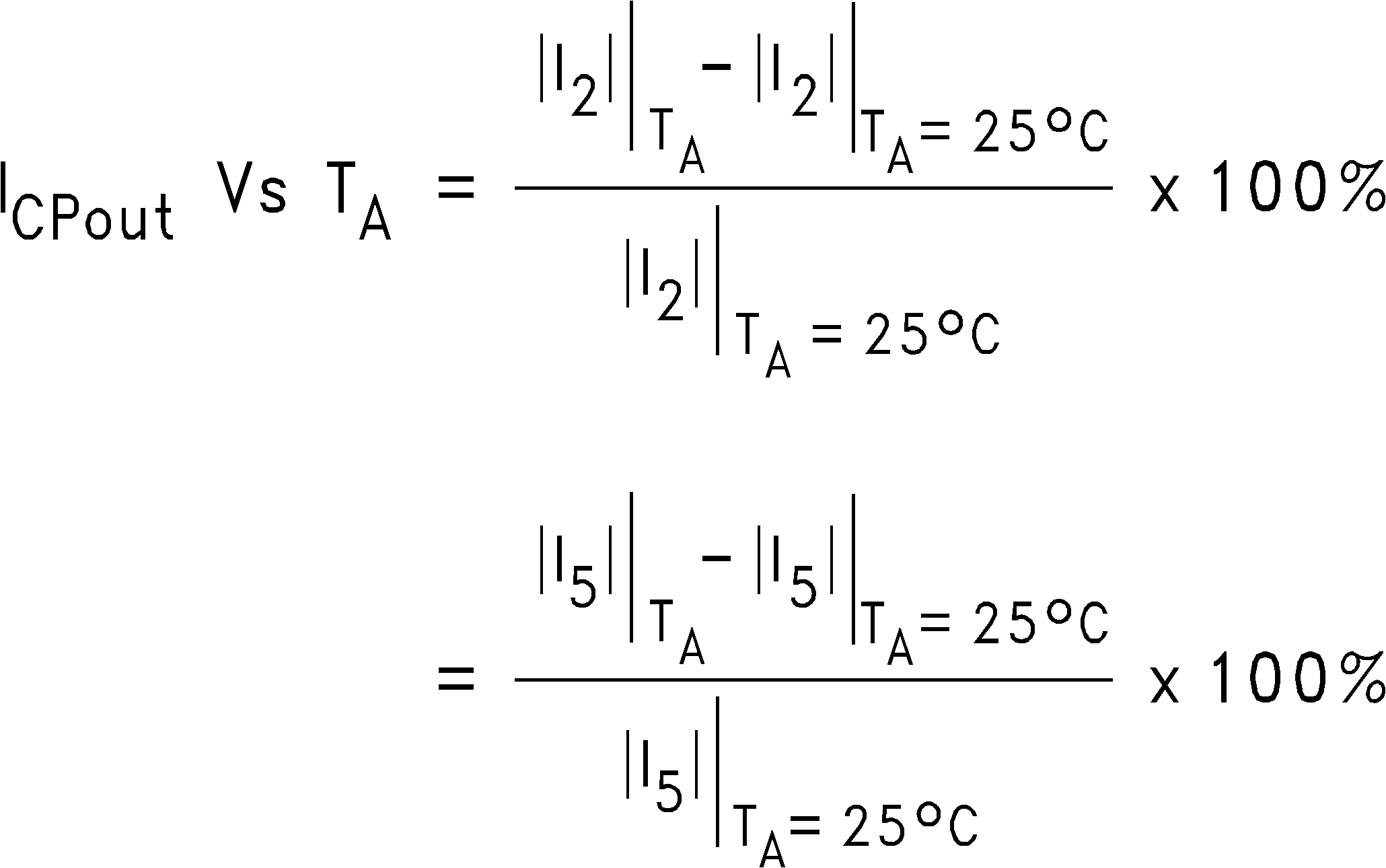
7.1.3 Charge Pump Output Current Magnitude Variation vs. Ambient Temperature
7.2 Differential Voltage Measurement Terminology
The differential voltage of a differential signal can be described by two different definitions causing confusion when reading datasheets or communicating with other engineers. This section will address the measurement and description of a differential signal so that the reader will be able to understand and discern between the two different definitions when used.
The first definition used to describe a differential signal is the absolute value of the voltage potential between the inverting and non-inverting signal. The symbol for this first measurement is typically VID or VOD depending on if an input or output voltage is being described.
The second definition used to describe a differential signal is to measure the potential of the non-inverting signal with respect to the inverting signal. The symbol for this second measurement is VSS and is a calculated parameter. Nowhere in the IC does this signal exist with respect to ground, it only exists in reference to its differential pair. VSS can be measured directly by oscilloscopes with floating references, otherwise this value can be calculated as twice the value of VOD as described in the first description.
Figure 8 illustrates the two different definitions side-by-side for inputs and Figure 9 illustrates the two different definitions side-by-side for outputs. The VID and VOD definitions show VA and VB DC levels that the non-inverting and inverting signals toggle between with respect to ground. VSS input and output definitions show that if the inverting signal is considered the voltage potential reference, the non-inverting signal voltage potential is now increasing and decreasing above and below the non-inverting reference. Thus the peak-to-peak voltage of the differential signal can be measured.
VID and VOD are often defined as volts (V) and VSS is often defined as volts peak-to-peak (VPP).
 Figure 8. Two Different Definitions for Differential Input Signals
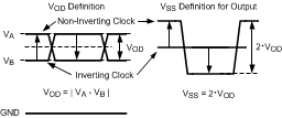 Figure 9. Two Different Definitions for Differential Output Signals
See AN-912, Common Data Transmission Parameters and their Definitions SNLA036, for more information.