-
TLV803E, TLV809E, TLV810E Low Power 250-nA IQ and Small Size Supply Voltage Supervisors
- 1 Features
- 2 Applications
- 3 Description
- 4 Revision History
- 5 Device Comparison
- 6 Pin Configuration and Functions
- 7 Specifications
- 8 Detailed Description
- 9 Application and Implementation
- 10Power Supply Recommendations
- 11Layout
- 12Device and Documentation Support
- 13Mechanical, Packaging, and Orderable Information
- IMPORTANT NOTICE
TLV803E, TLV809E, TLV810E Low Power 250-nA IQ and Small Size Supply Voltage Supervisors
1 Features
- Ensured RESET/RESET for VDD = 0.7 V to 6 V
- Fixed time delay: 40 µs, 10 ms, 50 ms, 100 ms, 200 ms, 400 ms
- Supply current (IDD): 250 nA (typical)
- 1 µA (maximum for VDD = 3.3 V)
- Output topology:
- TLV809E: push-pull, active-low
- TLV803E: open-drain, active-low
- TLV810E: push-pull, active-high
- Under voltage detection:
- High accuracy: ±0.5% (typical)
- (VIT–): 1.7 V, 1.8 V, 1.9 V, 2.25V, 2.4 V, 2.64 V,
2.93 V, 3.08 V, 3.3V, 4.2V, 4.38 V, 4.55V, 4.63 V
- Package:
- SOT23-3 (DBZ) (with pin 1 = GND)
- SOT23-3 (DBZ) (with pin 1 = RESET/RESET)
- SOT23-3 (DBZ) (with pin 3 = GND)
- SC-70 (DCK)
- X2SON-5 (DPW)
- Temperature range: –40°C to +125°C
- Pin-to-pin compatible with MAX803/809/810, APX803/809/810
3 Description
The TLV803E, TLV809E, and TLV810E are enhanced alternatives to the TLV803, TLV853, TLV809, LM809, TPS3809 and TLV810. TLV80xE and TLV81xE offer low quiescent current IQ, higher accuracy, wider temperature range, and lower power-on-reset (VPOR) for increased system reliability.
The TLV80xE and TLV81xE family are low
IQ (250 nA typical, 1 µA max), voltage supervisory circuits (reset IC) that
monitor VDD voltage level. These devices initiate a reset signal whenever supply voltage VDD
drops below the factory programmed falling threshold voltage, VIT–. The reset
output remains low for a fixed reset time delay tD after the VDD voltage rises
above the rising voltage threshold (VIT+) which is equivalent to the falling
threshold voltage (VIT-) plus hysteresis
(VHYS).
These devices have integrated glitch immunity to ignore fast transients on the VDD pin. The low IQ and high accuracy (±0.5% typical) makes these voltage supervisors ideal for use in low-power and portable applications. The TLV80xE and TLV81xE devices are specified to have the defined output logic state for supply voltages down to VPOR = 0.7 V. The TLV80xE and TLV81xE devices are available in industry standard 3-pin SOT23 (DBZ) and SC70 (DCK) packages and very compact X2SON (DPW) package.
| PART NUMBER | PACKAGE | BODY SIZE (NOM) |
|---|---|---|
| TLV803E, TLV809E, TLV810E | SOT-23 (3) | 2.90 mm × 1.30 mm |
| SC-70 (3) | 2.00 mm × 1.25 mm | |
| X2SON (5) | 0.8 mm x 0.8 mm |
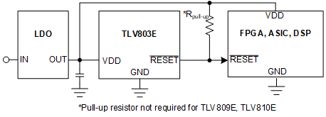
 Typical
Application
Typical
Application4 Revision History
Changes from Revision I (Feb 2021) to Revision J (May 2021)
- Updated Device Naming Nomenclature figure by adding Pinout Indicator (DBZ Package Only) from Pinout Indicator Go
- Updated pin numbering of Figure 6-5 (X2SON) package and updated Pin Functions TableGo
- Updated X2SON (DPW) Layout ExampleGo
Changes from Revision H (December 2020) to Revision I (February 2021)
- Remove duplicate package.Go
Changes from Revision G (October 2020) to Revision H (December 2020)
- Added Reset time delay variant F specificationGo
Changes from Revision F (June 2020) to Revision G (October 2020)
- Updated the numbering format for tables, figures and cross-references throughout the document.Go
- Added additional threshold voltages (VIT-) and new package information Go
- Updated Device Naming Nomenclature figure to include (DBZ) V pinout option Go
- Added new (DBZ) package option (Pin 3 = GND, V pinout) and updated Pin Functions TableGo
- Added layout example for (DBZ) V pinout packageGo
- Modified Device Naming Convention table to include additional threshold voltages (VIT-), reset time delay options and pinout indicator optionsGo
Changes from Revision E (April 2020) to Revision F (June 2020)
Changes from Revision D (February 2020) to Revision E (April 2020)
- Added X2SON (DPW) package option Go
Changes from Revision C (November 2019) to Revision D (February 2020)
Changes from Revision B (July 2019) to Revision C (November 2019)
- Changed device status from Advance Information to Production DataGo
Changes from Revision A (June 2019) to Revision B (July 2019)
- Updated advance information data sheet Go
Changes from Revision * (August 2018) to Revision A (June 2019)
- Changed data sheet status from Product Preview to Advanced Information Go