• Menu
  • Product
  • Email
  • PDF
  • Order now
  • TPS62864/6 2.4-V to 5.5-V Input, 4-A and 6-A Synchronous Step-Down Converter with I2C Interface in WCSP Package

    • SLVSEI1C June   2019  – October 2020 TPS62864 , TPS62866

      PRODUCTION DATA  

  • CONTENTS
  • SEARCH
  • TPS62864/6 2.4-V to 5.5-V Input, 4-A and 6-A Synchronous Step-Down Converter with I2C Interface in WCSP Package
  1. 1 Features
  2. 2 Applications
  3. 3 Description
  4. 4 Revision History
  5. 5 Device Options
  6. 6 Pin Configuration and Functions
  7. 7 Specifications
    1. 7.1 Absolute Maximum Ratings
    2. 7.2 ESD Ratings
    3. 7.3 Recommended Operating Conditions
    4. 7.4 Thermal Information
    5. 7.5 Electrical Characteristics
    6. 7.6 I2C InterfaceTiming Characteristics
    7. 7.7 Typical Characteristics
  8. 8 Detailed Description
    1. 8.1 Overview
    2. 8.2 Functional Block Diagram
    3. 8.3 Feature Description
      1. 8.3.1 Power Save Mode
      2. 8.3.2 Forced PWM Mode
      3. 8.3.3 Start-up
      4. 8.3.4 Switch Current Limit and HICCUP Short-Circuit Protection
      5. 8.3.5 Undervoltage Lockout (UVLO)
      6. 8.3.6 Thermal Warning and Shutdown
    4. 8.4 Device Functional Modes
      1. 8.4.1 Enable and Disable (EN)
      2. 8.4.2 Output Discharge
      3. 8.4.3 Start-up Output Voltage and I2C Slave Address Selection (VSET)
      4. 8.4.4 Select Output Voltage Registers (VID)
      5. 8.4.5 Power Good (PG)
    5. 8.5 Programming
      1. 8.5.1 Serial Interface Description
      2. 8.5.2 Standard-, Fast-, and Fast-Mode Plus Protocol
      3. 8.5.3 HS-Mode Protocol
      4. 8.5.4 I2C Update Sequence
      5. 8.5.5 I2C Register Reset
    6. 8.6 Register Map
      1. 8.6.1 Slave Address Byte
      2. 8.6.2 Register Address Byte
      3. 8.6.3 VOUT Register 1
      4. 8.6.4 VOUT Register 2
      5. 8.6.5 CONTROL Register
      6. 8.6.6 STATUS Register
  9. 9 Application and Implementation
    1. 9.1 Application Information
    2. 9.2 Typical Applications
      1. 9.2.1 6-A Output Current Application
        1. 9.2.1.1 Design Requirements
        2. 9.2.1.2 Detailed Design Procedure
          1. 9.2.1.2.1 Custom Design With WEBENCH® Tools
          2. 9.2.1.2.2 Setting The Output Voltage
          3. 9.2.1.2.3 Output Filter Design
          4. 9.2.1.2.4 Inductor Selection
          5. 9.2.1.2.5 Capacitor Selection
        3. 9.2.1.3 Application Curves
      2. 9.2.2 Smaller Application Solution
        1. 9.2.2.1 Design Requirements
        2. 9.2.2.2 Application Curves
  10. 10Power Supply Recommendations
  11. 11Layout
    1. 11.1 Layout Guidelines
    2. 11.2 Layout Example
    3. 11.3 Thermal Considerations
  12. 12Device and Documentation Support
    1. 12.1 Device Support
      1. 12.1.1 Third-Party Products Disclaimer
    2. 12.2 Documentation Support
      1. 12.2.1 Related Documentation
    3. 12.3 Support Resources
    4. 12.4 Receiving Notification of Documentation Updates
    5. 12.5 Trademarks
    6. 12.6 Electrostatic Discharge Caution
    7. 12.7 Glossary
  13. 13Mechanical, Packaging, and Orderable Information
  14. IMPORTANT NOTICE
search No matches found.
  • Full reading width
    • Full reading width
    • Comfortable reading width
    • Expanded reading width
  • Card for each section
  • Card with all content


DATA SHEET

TPS62864/6 2.4-V to 5.5-V Input, 4-A and 6-A Synchronous Step-Down Converter with I2C Interface in WCSP Package

1 Features

  • 7-mΩ and 6.5-mΩ internal power MOSFETs
  • >90% efficiency (0.9-V output)
  • DCS-control topology for fast transient response
  • 1% output voltage accuracy
  • 4-µA operating quiescent current
  • 2.4-V to 5.5-V input voltage range
  • 2.4-MHz switching frequency
  • Selection by external resistor
    • Start-up output voltage
    • I2C slave address
  • Selection by I2C interface
    • Power save mode or forced PWM mode
    • Output discharge
    • Hiccup or latching short-circuit protection
    • Output voltage ramp speed
  • VID pin for dynamic voltage scaling (DVS)
  • Thermal pre-warning and thermal shutdown
  • Power good indicator pin option
  • I2C-compatible interface up to 3.4 Mbps
  • Available in 1.05-mm x 1.78-mm x 0.5-mm 15-pin WCSP package with 0.35-mm pitch
  • Create a custom design using the TPS62866 with the WEBENCH® Power Designer

2 Applications

  • Core supply for FPGAs, CPUs, ASICs or video chipsets
  • Camera modules
  • Solid-state drives
  • Optical modules

3 Description

The TPS62864 and TPS62866 devices are high-frequency synchronous step-down converters with I2C interface which provide an efficient, adaptive, and high power-density solution. At medium to heavy loads, the converter operates in PWM mode and automatically enters Power Save Mode operation at light load to maintain high efficiency over the entire load current range. The device can also be forced in PWM mode operation for smallest output voltage ripple. Together with its DCS-control architecture, excellent load transient performance and tight output voltage accuracy are achieved. Via the I2C interface and a dedicated VID pin, the output voltage is quickly adjusted to adapt the power consumption of the load to the ever-changing performance needs of the application.

Device Information
PART NUMBER PACKAGE(1) BODY SIZE (NOM)
TPS62864 WCSP (15) 1.05 x 1.78 x 0.5 mm
TPS62866
(1) For all available packages, see the orderable addendum at the end of the data sheet.
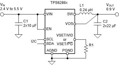
GUID-5F084025-9514-4072-8654-4D589F25AC8E-low.gifTypical Application
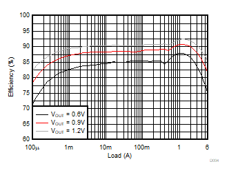
GUID-88928BFA-83D6-4044-9D71-76898177E599-low.gifEfficiency at VIN = 3.3 V


Texas Instruments

© Copyright 1995-2025 Texas Instruments Incorporated. All rights reserved.
Submit documentation feedback | IMPORTANT NOTICE | Trademarks | Privacy policy | Cookie policy | Terms of use | Terms of sale