-
TPS6306x High Input Voltage, Buck-Boost Converter With 2-A Switch Current
- 1 Features
- 2 Applications
- 3 Description
- 4 Revision History
- 5 Device Comparison
- 6 Pin Configuration and Functions
- 7 Specifications
- 8 Detailed Description
- 9 Application and Implementation
- 10Power Supply Recommendations
- 11Layout
- 12Device and Documentation Support
- 13Mechanical, Packaging, and Orderable Information
- IMPORTANT NOTICE
TPS6306x High Input Voltage, Buck-Boost Converter With 2-A Switch Current
1 Features
- Input voltage range: 2.5 V to 12 V
- Efficiency: Up to 93%
- Output current at 5 V (VIN < 10 V):
2 A in buck mode - Output current at 5 V (VIN > 4
V):
1.3 A in boost mode - Automatic transition between step down and boost mode
- Typical device quiescent current: < 30 μA
- Fixed and adjustable output voltage options from 2.5 V to 8 V
- Power save mode for improved efficiency at low output power
- Forced fixed-frequency operation at 2.4 MHz and synchronization possible
- Power good output
- Buck-Boost Overlap Control™
- Load disconnect during shutdown
- Overtemperature protection
- Overvoltage protection
2 Applications
- Dual Li-ion application
- Digital still cameras (DSC) and camcorders
- Notebook computer
- Industrial metering equipment
- Ultra mobile PCs and mobile internet devices
- Personal medical products
- High-power LEDs
3 Description
The TPS6306x devices provide a power supply solution for products powered by either three-cell up to six-cell alkaline, NiCd or NiMH battery, or a one-cell or dual-cell Li-Ion or Li-polymer battery. Output currents can go as high as 2 A while using a dual-cell Li-Ion or Li-polymer battery, and discharge to 5 V or lower. The buck-boost converter is based on a fixed frequency, pulse width modulation (PWM) controller using synchronous rectification to obtain maximum efficiency. At low load currents, the converter enters power save mode to maintain high efficiency over a wide load current range. The power save mode can be disabled, forcing the converter to operate at a fixed switching frequency. The maximum average current in the switches is limited to a typical value of 2.25 A. The output voltage is programmable using an external resistor divider, or is fixed internally on the chip. The converter can be disabled to minimize battery drain. During shutdown, the load disconnects from the battery.
The devices are available in a 3 mm × 3 mm, 10-pin, WSON (DSC) package.
| PART NUMBER | PACKAGE | BODY SIZE (NOM) |
|---|---|---|
| TPS63060 | WSON (10) | 3.00 mm × 3.00 mm |
| TPS63061 |
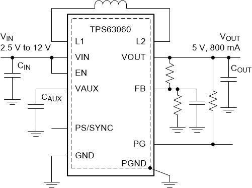
 Simplified Application
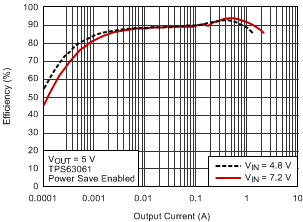
 Efficiency vs Output Current
4 Revision History
Changes from Revision B (December 2014) to Revision C (September 2020)
- Updated the numbering format for tables, figures, and cross-references throughout the documentGo
- Changed Application From: DSCs and Camcorders To: Digital Still Cameras (DSC) and CamcordersGo
- Deleted PowerPAD™ package from the Description Go
- Changed the Typical Application Schematic Go
- Removed PACKAGE MARKING from the Device Comparison Table Go
- Changed From: PowerPAD™ To: Exposed Thermal Pad in the Pin Functions tableGo
- Changed L1 and L2 values in the Absolute Maximum Ratings tableGo
- Deleted Machine model (MM) from the ESD Ratings tableGo
- Added "Thermal shutdown" and "Thermal Shutdown hysteresis" to the Electrical Characteristics tableGo
- Deleted "Overtemperature protection" and "Overtemperature hysteresis" from the Electrical Characteristics tableGo
- Added "Maximum reverse current" to the Electrical Characteristics tableGo
- Added condition footnote to Electrical Characteristics tableGo
- Changed the Overview sectionGo
- Changed Figure 8-1 Title From: TPS63061 Fixed Output To: TPS63060 AdjustableGo
- Changed Figure 8-2 Title From: TPS63060 Adjustable To: TPS63061 Fixed OutputGo
- Split the Soft-Start Function and Short-Circuit Protection into two separate sectionsGo
- Moved Synchronization from the Power-Save Mode section into a separate sectionGo
- Changed C2 (2 x 10 µF) To: C1 (2 x 10 µF) in Figure 9-1 Go
- Deleted two graphs "Output Current vs Input Voltage" and "Output Current vs Input Voltage" from the Application Curves Go
Changes from Revision A (February 2012) to Revision B (December 2014)
- Added ESD Ratings table, Feature Description section, Device Functional Modes section, Application and Implementation section, Power Supply Recommendations section, Layout section, Device and Documentation Support section, and Mechanical, Packaging, and Orderable Information sectionGo