TPS54325 4.5-V to 18-V, 3-A Output Synchronous Step Down Switcher with Integrated FET
1 Features
- D-CAP2™ Mode Enables Fast Transient Response
- Low Output Ripple and Allows Ceramic Output Capacitor
- Wide VCC Input Voltage Range: 4.5 V to 18 V
- Wide VIN Input Voltage Range: 2.0 V to 18 V
- Output Voltage Range: 0.76 V to 5.5 V
- Highly Efficient Integrated FET’s Optimized for Lower Duty Cycle Applications – 120 mΩ (High Side) and 70 mΩ (Low Side)
- High Efficiency, less than 10 μA at shutdown
- High Initial Bandgap Reference Accuracy
- Adjustable Soft Start
- Pre-Biased Soft Start
- 700-kHz Switching Frequency (fSW)
- Cycle By Cycle Over Current Limit
- Power Good Output
2 Applications
- Wide Range of Applications for Low Voltage System
- Digital TV Power Supply
- High Definition Blu-ray Disc™ Players
- Networking Home Terminal
- Digital Set Top Box (STB)
3 Description
The TPS54325 device is an adaptive on-time D-CAP2™ mode synchronous buck converter. The TPS54325 device enables system designers to complete the suite of various end equipment’s power bus regulators with a cost effective, low component count, low standby current solution.
The main control loop for the TPS54325 uses the D-CAP2™ mode control which provides a very fast transient response with no external components. The TPS54325 also has a proprietary circuit that enables the device to adapt to both low equivalent series resistance (ESR) output capacitors, such as POSCAP or SP-CAP, and ultra-low ESR ceramic capacitors. The device operates from 4.5-V to 18-V VCC input , and from 2.0-V to 18-V VIN input power supply voltage. The output voltage can be programmed between 0.76 V and 5.5 V. The device also features an adjustable slow start time and a power good function. The TPS54325 is available in the 14 pin HTSSOP package, and designed to operate from –40°C to 85°C.
Device Information(1)
| PART NUMBER | PACKAGE | BODY SIZE (NOM) |
|---|---|---|
| TPS54325 | HTSSOP (14) | 5.00 mm × 4.40 mm |
- For all available packages, see the orderable addendum at the end of the datasheet.
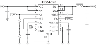
4 Simplified Schematic
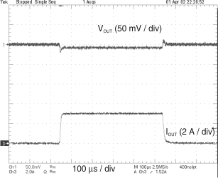
Load Transient Response
5 Revision History
Changes from E Revision (January 2014) to F Revision
- Added, updated, or renamed the following sections: Device Information Table, Application and Implementation; Power Supply Recommendations; Layout; Device and Documentation Support; Mechanical, Packaging, and Ordering InformationGo
Changes from D Revision (January 2012) to E Revision
- Changed text in the Bootstrap Capacitor Selection from "between the VREG5 to GND pin for proper operation" to "between the VBST to SW pin for proper operationGo
Changes from C Revision (July 2011) to D Revision
Changes from B Revision (March 2011) to C Revision
- Changed EN high-level input voltage from min of 2.0 V to min of 1.6 VGo
- Changed EN low-level input voltage from max of 0.48 V to max of 0.4 VGo
Changes from * Revision (May 2009) to A Revision
- Changed TA, for the current limit, Iocl, From: 25°C to –40°C To: 85°C and 3.5 A was added at the MIN valueGo
6 Pin Configuration and Functions

Pin Functions
| PIN | I/O | DESCRIPTION | |
|---|---|---|---|
| NAME | NO. | ||
| VO | 1 | I | Connect to output of converter. This terminal is used for On-Time Adjustment. |
| VFB | 2 | I | Converter feedback input. Connect with feedback resistor divider. |
| VREG5 | 3 | O | 5.5 V power supply output. A capacitor (typical 1μF) should be connected to GND. |
| SS | 4 | I | Soft-start control. A external capacitor should be connected to GND. |
| GND | 5 | –– | Signal ground pin |
| PG | 6 | O | Open drain power good output |
| EN | 7 | I | Enable control input |
| PGND1, PGND2 | 8, 9 | –– | Ground returns for low-side MOSFET. Also serve as inputs of current comparators. Connect PGND and GND strongly together near the IC. |
| SW1, SW2 | 10, 11 | O | Switch node connection between high-side NFET and low-side NFET. Also serve as inputs to current comparators. |
| VBST | 12 | O | Supply input for high-side NFET gate driver (boost terminal). Connect capacitor from this pin to respective SW1, SW2 terminals. An internal PN diode is connected between VREG5 to VBST pin. |
| VIN | 13 | I | Power input and connected to high side NFET drain |
| VCC | 14 | I | Supply input for 5 V internal linear regulator for the control circuitry |
| PowerPAD™ | –– | –– | Thermal pad of the package. Must be soldered to achieve appropriate dissipation. Should be connected to PGND. |