-
TPS6500xx 2.25-MHz Step-Down Converter With Dual Low Dropouts and Supply Voltage Supervisor
- 1 Features
- 2 Applications
- 3 Description
- 4 Revision History
- 5 Description (continued)
- 6 Device Options
- 7 Pin Configuration and Functions
- 8 Specifications
- 9 Detailed Description
- 10Application and Implementation
- 11Power Supply Recommendations
- 12Layout
- 13Device and Documentation Support
- 14Mechanical, Packaging, and Orderable Information
- IMPORTANT NOTICE
TPS6500xx 2.25-MHz Step-Down Converter With Dual Low Dropouts and Supply Voltage Supervisor
1 Features
- Step-Down Converters:
- VIN Range From 2.3 V to 6 V
- Spread Spectrum Clock (SSC) Generation for Reduced EMI
- 2.25-MHz Fixed Frequency Operation
- 600-mA or 1-A (TPS650061) Output Current
- Low Dropouts (LDOs):
- VIN Range From 1.6 V to 6 V
- Adjustable Output Voltage
- Up to 300-mA Output Current
- Separate Power Inputs and Enables
- Supply Voltage Supervisor (TPS65001)
- Manual Reset Input for Push Button
- Adjustable Reset Time
- Adjustable Reset Voltage
- 3-mm × 3-mm 16-Pin WQFN (TPS65000)
- 3-mm × 3-mm 20-Pin WQFN (TPS65001)
2 Applications
- Points-of-Load
- Embedded Processor Power
- Cell Phones
- Smart Phones
- PDAs
- Pocket PCs
- Portable Media Players
3 Description
The TPS6500xx devices are single-chip power management (PWM) ICs for portable applications. Both devices combine a single step-down converter with two low-dropout (LDO) regulators. The step-down converter enters a low-power mode at light load for maximum efficiency across the widest possible range of load currents. For low-noise applications, the devices can be forced into fixed-frequency PWM through a pin. The step-down converter is small because of its small inductor and capacitors. The step-down converter has power good status output for sequencing. The LDOs can supply 300 mA and operate with an input voltage range from 1.6 V to 6 V. A step-down converter or main battery can power the LDOs directly. The step-down converter and the LDOs have separate voltage inputs that enable maximum design and sequencing flexibility.
Device Information(1)
| PART NUMBER | PACKAGE | BODY SIZE (NOM) |
|---|---|---|
| TPS65000, TPS650001, TPS650003, TPS650006 |
WQFN (16) | 3.00 mm × 3.00 mm |
| TPS65001, TPS650061 |
WQFN (20) | 3.00 mm × 3.00 mm |
- For all available packages, see the orderable addendum at the end of the data sheet.
4 Revision History
Changes from B Revision (August 2010) to C Revision
- Added ESD Ratings table, Feature Description section, Device Functional Modes, Application and Implementation section, Power Supply Recommendations section, Layout section, Device and Documentation Support section, and Mechanical, Packaging, and Orderable Information sectionGo
Changes from A Revision (October 2009) to B Revision
- In the Ordering Information Table, changed the SVS column From: Included To: N/A for devices TPS650001, TPS650003, TPS650006 Go
Changes from * Revision (June 2009) to A Revision
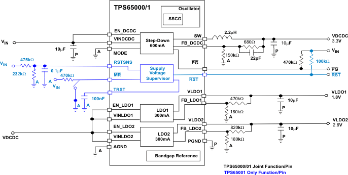
- Changed the PG pin connection From: VDCDC To: VIN in the application circuit.Go
- Changed resistor values for VLDO1 and VLDO2 in the application circuit.Go
- Changed the configuration of the PG and RST pins in the application circuitGo
- Added Note 2: to the Electrical Characteristics table.Go
- Changed Figure 1 title From: EFFICIENCY (DCDC PFM Mode) To: EFFICIENCY (DCDC 600mA PFM Mode)Go
- Changed Figure 2 title From: EFFICIENCY (DCDC PFM Mode) To: EFFICIENCY (DCDC 600mA PFM Mode)Go
- Added Figure 3, EFFICIENCY (DCDC PWM Mode)Go
- Added Figure 4, EFFICIENCY (DCDC PWM Mode)Go
- Changed the configuration of the PG pin in Figure 24 Go
- Changed the PG pin connection From: VDCDC To: VIN in Figure 31.Go
- Changed the configuration of the PG and RST pins in Figure 31 Go
- Added Figure 32, Typical TPS650001 Application SchematicGo
- Added Figure 33, Typical TPS650061 Application SchematicGo
5 Description (continued)
The TPS65001 extends functionality by adding a supply voltage supervisor (SVS). To maximize the flexibility of the SVS, the reset voltage is set with two external resistors and the reset time is set by a small external capacitor. For external control, the SVS can use its active-low manual reset input to connect to a push button.
The TPS65000 is available in a 16-pin leadless package (3 mm × 3 mm QFN). The TPS65001 is available in a 20-pin leadless package (3 mm × 3 mm QFN).
