• Menu
  • Product
  • Email
  • PDF
  • Order now
  • UCC21750-Q1 10-A Source/Sink Reinforced Isolated Single Channel Gate Driver for SiC/IGBT with Active Protection, Isolated Analog Sensing and High-CMTI

    • SLUSDH9D September   2019  – November 2023 UCC21750-Q1

      PRODUCTION DATA  

  • CONTENTS
  • SEARCH
  • UCC21750-Q1 10-A Source/Sink Reinforced Isolated Single Channel Gate Driver for SiC/IGBT with Active Protection, Isolated Analog Sensing and High-CMTI
  1.   1
  2. 1 Features
  3. 2 Applications
  4. 3 Description
  5. 4 Revision History
  6. 5 Pin Configuration and Functions
  7. 6 Specifications
    1. 6.1  Absolute Maximum Ratings
    2. 6.2  ESD Ratings
    3. 6.3  Recommended Operating Conditions
    4. 6.4  Thermal Information
    5. 6.5  Power Ratings
    6. 6.6  Insulation Specifications
    7. 6.7  Safety Limiting Values
    8. 6.8  Electrical Characteristics
    9. 6.9  Safety-Related Certifications
    10. 6.10 Switching Characteristics
    11. 6.11 Insulation Characteristics Curves
    12. 6.12 Typical Characteristics
  8. 7 Parameter Measurement Information
    1. 7.1 Propagation Delay
      1. 7.1.1 Regular Turn-OFF
    2. 7.2 Input Deglitch Filter
    3. 7.3 Active Miller Clamp
      1. 7.3.1 Internal On-Chip Active Miller Clamp
    4. 7.4 Undervoltage Lockout (UVLO)
      1. 7.4.1 VCC UVLO
      2. 7.4.2 VDD UVLO
    5. 7.5 Desaturation (DESAT) Protection
      1. 7.5.1 DESAT Protection with Soft Turn-OFF
  9. 8 Detailed Description
    1. 8.1 Overview
    2. 8.2 Functional Block Diagram
    3. 8.3 Feature Description
      1. 8.3.1  Power Supply
      2. 8.3.2  Driver Stage
      3. 8.3.3  VCC and VDD Undervoltage Lockout (UVLO)
      4. 8.3.4  Active Pulldown
      5. 8.3.5  Short Circuit Clamping
      6. 8.3.6  Internal Active Miller Clamp
      7. 8.3.7  Desaturation (DESAT) Protection
      8. 8.3.8  Soft Turn-Off
      9. 8.3.9  Fault (FLT, Reset, and Enable (RST/EN)
      10. 8.3.10 Isolated Analog to PWM Signal Function
    4. 8.4 Device Functional Modes
  10. 9 Applications and Implementation
    1. 9.1 Application Information
    2. 9.2 Typical Application
      1. 9.2.1 Design Requirements
      2. 9.2.2 Detailed Design Procedure
        1. 9.2.2.1 Input Filters for IN+, IN–, and RST/EN
        2. 9.2.2.2 PWM Interlock of IN+ and IN–
        3. 9.2.2.3 FLT, RDY, and RST/EN Pin Circuitry
        4. 9.2.2.4 RST/EN Pin Control
        5. 9.2.2.5 Turn-On and Turn-Off Gate Resistors
        6. 9.2.2.6 Overcurrent and Short Circuit Protection
        7. 9.2.2.7 Isolated Analog Signal Sensing
          1. 9.2.2.7.1 Isolated Temperature Sensing
          2. 9.2.2.7.2 Isolated DC Bus Voltage Sensing
        8. 9.2.2.8 Higher Output Current Using an External Current Buffer
      3. 9.2.3 Application Curves
  11. 10Power Supply Recommendations
  12. 11Layout
    1. 11.1 Layout Guidelines
    2. 11.2 Layout Example
  13. 12Device and Documentation Support
    1. 12.1 Device Support
      1. 12.1.1 Third-Party Products Disclaimer
    2. 12.2 Documentation Support
      1. 12.2.1 Related Documentation
    3. 12.3 Receiving Notification of Documentation Updates
    4. 12.4 Support Resources
    5. 12.5 Trademarks
    6. 12.6 Electrostatic Discharge Caution
    7. 12.7 Glossary
  14. 13Mechanical, Packaging, and Orderable Information
  15. IMPORTANT NOTICE
search No matches found.
  • Full reading width
    • Full reading width
    • Comfortable reading width
    • Expanded reading width
  • Card for each section
  • Card with all content


Data Sheet

UCC21750-Q1 10-A Source/Sink Reinforced Isolated Single Channel Gate Driver
for SiC/IGBT with Active Protection, Isolated Analog Sensing and High-CMTI

1 Features

  • 5.7-kVRMS single channel isolated gate driver
  • AEC-Q100 qualified for automotive applications
    • Device temperature grade 1: -40°C to +125°C ambient operating temperature range
    • Device HBM ESD classification level 3A
    • Device CDM ESD classification level C3
  • SiC MOSFETs and IGBTs up to 2121Vpk
  • 33-V maximum output drive voltage (VDD – VEE)
  • ±10-A drive strength and split output
  • 150-V/ns minimum CMTI
  • 200-ns response time fast DESAT protection
  • 4-A Internal active miller clamp
  • 400-mA soft turn-off when fault happens
  • Isolated analog sensor with PWM output for
    • Temperature sensing with NTC, PTC or thermal diode
    • High voltage DC-link or phase voltage
  • Alarm FLT on overcurrent and reset from RST/EN
  • Fast enable and disable response on RST/EN
  • Reject < 40-ns noise transient and pulse on input pins
  • 12-V VDD UVLO with power good on RDY
  • Inputs/outputs with over/under-shoot transient voltage immunity up to 5 V
  • 130-ns (maximum) propagation delay and 30-ns (maximum) pulse/part skew
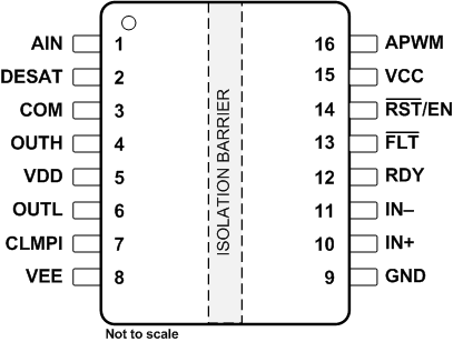
  • SOIC-16 DW package with creepage and clearance distance > 8 mm
  • Operating junction temperature –40°C to 150°C
  • Safety-related certifications:
    • Reinforced insulation per DIN EN IEC 60747-17 (VDE 0884-17)
    • UL 1577 component recognition program

2 Applications

  • Traction inverter for EVs
  • On-board charger and charging pile
  • DC/DC converter for HEV/EVs

3 Description

The UCC21750-Q1 is a galvanic isolated single channel gate driver designed for SiC MOSFETs and IGBTs up to 2121-V DC operating voltage with advanced protection features, best-in-class dynamic performance and robustness. The UCC21750-Q1 has up to ±10-A peak source and sink current.

The input side is isolated from the output side with SiO2 capacitive isolation technology, supporting up to 1.5-kVRMS working voltage, 12.8-kVPK surge immunity with longer than 40 years Isolation barrier life, as well as providing low part-to-part skew, and > 150-V/ns common mode noise immunity (CMTI).

The UCC21750-Q1 includes the state-of-art protection features, such as fast overcurrent and short circuit detection, shunt current sensing support, fault reporting, active miller clamp, and input and output side power supply UVLO to optimize SiC and IGBT switching behavior and robustness. The isolated analog to PWM sensor can be used for easier temperature or voltage sensing, further increasing the drivers' versatility and simplifying the system design effort, size, and cost.

Device Information
PART NUMBER PACKAGE(1) BODY SIZE (NOM)
UCC21750-Q1 DW SOIC-16 10.3 mm × 7.5 mm
(1) For all available packages, see the orderable addendum at the end of the data sheet.
Device Pin Configuration
GUID-D6D4F95A-8BC2-4CD1-97E9-B519E7136F9C-low.gif


Texas Instruments

© Copyright 1995-2025 Texas Instruments Incorporated. All rights reserved.
Submit documentation feedback | IMPORTANT NOTICE | Trademarks | Privacy policy | Cookie policy | Terms of use | Terms of sale