-
TPS254900-Q1 Automotive USB Host Charger With Short-to-VBATT Protection
- 1 Features
- 2 Applications
- 3 Description
- 4 Revision History
- 5 Pin Configuration and Functions
- 6 Specifications
- 7 Parameter Measurement Information
-
8 Detailed Description
- 8.1 Overview
- 8.2 Functional Block Diagram
- 8.3 Feature Description
- 8.4 Device Functional Modes
- 9 Application and Implementation
- 10Power Supply Recommendations
- 11Layout
- 12Device and Documentation Support
- 13Mechanical, Packaging, and Orderable Information
- IMPORTANT NOTICE
TPS254900-Q1 Automotive USB Host Charger With Short-to-VBATT Protection
1 Features
- AEC-Q100 Qualified With the Following Results:
- Device HBM ESD Classification Level H2
- Device CDM ESD Classification Level C5
- 4.5-V to 6.5-V Input Operating Range
- Integrated 45-mΩ (typ.) High-Side MOSFET
- 3-A Maximum Continuous Output Current
- VBUS ±5% Cable Compensation Accuracy at Connector
- Supports USB BC 1.2 CDP and SDP Modes
- Short-to-Battery Protection on OUT, DP_IN, and DM_IN Pins
- DP_IN and DM_IN IEC 61000-4-2 Rated
- ±8-kV Contact and ±15-kV Air Discharge
- 20-Pin QFN (3-mm × 4-mm) Package
2 Applications
- Automotive USB Charging Ports (Host and Hubs)
- Automotive USB Protection
3 Description
The TPS254900-Q1 device is a USB charging-port controller and power switch with short-to-battery protection. This feature provides protection on OUT, DM_IN and DP_IN. These three pins withstand voltage up to 18 V. The internal MOSFET turns off quickly when the short-to-battery condition occurs. Rapid turnoff is very important to protect the upstream dc-dc converter, processor, or hub data lines.
The TPS254900-Q1 45-mΩ power switch has two selectable, adjustable current limits that support port power management by changing to a lower current limit when adjacent ports are experiencing heavy loads. This is important in systems with multiple ports and upstream power supplies with limited capacity.
The TPS254900-Q1 has a current-sense output that is able to control an upstream supply, which allows it to maintain 5 V at the USB port even with heavy charging currents. This feature is important in systems with long USB cables where significant voltage drops can occur with fast-charging portable devices.
A current monitor allows a system to monitor the load current in real time by monitoring the IMON voltage. The current monitor is very useful and can be used for dynamic port-power management.
The TPS254900-Q1 device also provides ESD protection capability per IEC 61000-4-2, level 4 on DP_IN and DM_IN.
Device Information(1)
| PART NUMBER | PACKAGE | BODY SIZE (NOM) |
|---|---|---|
| TPS254900-Q1 | WQFN (20) | 3.00 mm × 4.00 mm |
- For all available packages, see the orderable addendum at the end of the data sheet.
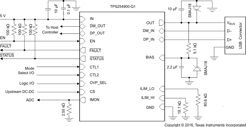
Schematic

4 Revision History
Changes from * Revision (September 2016) to A Revision
- Changed data sheet from PRODUCT PREVIEW to PRODUCTION DATAGo
5 Pin Configuration and Functions
Pin Functions
| PIN | TYPE(1) | DESCRIPTION | |
|---|---|---|---|
| NAME | NO. | ||
| BIAS | 12 | PWR | Used for IEC protection. Typically, connect a 2.2-µF capacitor and a transient-voltage suppressor (TVS) to ground and 5.1 kΩ to OUT. |
| CS | 6 | O | Linear cable compensation current. Connect to divider resistor of front-end dc-dc converter. |
| CTL1 | 8 | I | Logic-level control input for controlling the charging mode and the signal switches; see the Device Truth Table (TT). |
| CTL2 | 9 | I | Logic-level control input for controlling the charging mode and the signal switches; see the Device Truth Table (TT). |
| DM_IN | 14 | I/O | D– data line to downstream connector |
| DM_OUT | 4 | I/O | D– data line to upstream USB host controller |
| DP_IN | 13 | I/O | D+ data line to downstream connector |
| DP_OUT | 5 | I/O | D+ data line to upstream USB host controller |
| EN | 7 | I | Logic-level control input for turning the power and signal switches on or off. When EN is low, the device is disabled, and the signal and power switches are OFF. |
| FAULT | 18 | O | Active-low, open-drain output, asserted during overtemperature, overcurrent, and overvoltage conditions. |
| GND | 11 | — | Ground connection; should be connected externally to the thermal pad. |
| ILIM_HI | 20 | I | External resistor used to set the high current-limit threshold. |
| ILIM_LO | 19 | I | External resistor used to set the low current-limit threshold and the load-detection current threshold. |
| IMON | 1 | O | This pin sources a scaled-down ratio of current through the internal FET. A resistor from this pin to GND converts current to proportional voltage; used as an analog current monitor. |
| IN | 2,3 | PWR | Input supply voltage; connect a 0.1-µF or greater ceramic capacitor from IN to GND as close to the IC as possible. |
| OUT | 15,16 | PWR | Power-switch output |
| OVP_SEL | 10 | I | Logic-level control input for choosing the OUT overvoltage threshold. When OVP_SEL is low, V(OV_OUT_LOW) is active. When OVP_SEL is high, V(OV_OUT_HIGH) is active. |
| STATUS | 17 | O | Active-low open-drain output, asserted in load-detect conditions |
| Thermal pad | — | — | Thermal pad on the bottom of the package |