-
UCC21220, UCC21220A 4A, 6A, Dual-Channel Basic and Functional Isolated Gate Drivers with High Noise Immunity
- 1
- 1 Features
- 2 Applications
- 3 Description
- 4 Device Comparison Table
- 5 Pin Configuration and Functions
- 6 Specifications
- 7 Parameter Measurement Information
- 8 Detailed Description
-
9 Application and Implementation
- 9.1 Application Information
- 9.2
Typical Application
- 9.2.1 Design Requirements
- 9.2.2
Detailed Design Procedure
- 9.2.2.1 Designing INA/INB Input Filter
- 9.2.2.2 Select External Bootstrap Diode and its Series Resistor
- 9.2.2.3 Gate Driver Output Resistor
- 9.2.2.4 Estimating Gate Driver Power Loss
- 9.2.2.5 Estimating Junction Temperature
- 9.2.2.6 Selecting VCCI, VDDA/B Capacitor
- 9.2.2.7 Application Circuits with Output Stage Negative Bias
- 9.2.3 Application Curves
- 10Power Supply Recommendations
- 11Layout
- 12Device and Documentation Support
- 13Revision History
- 14Mechanical, Packaging, and Orderable Information
- IMPORTANT NOTICE
UCC21220, UCC21220A 4A, 6A, Dual-Channel Basic and Functional Isolated Gate Drivers with High Noise Immunity
1 Features
- Universal: dual low-side, dual high-side or half-bridge driver
- Supports basic and functional isolation
- CMTI greater than 125V/ns
- Up to 4A peak source, 6A peak sink output
- Switching
parameters:
- 33ns typical propagation delay
- 5ns maximum pulse-width distortion
- 10µs maximum VDD power-up delay
- Up to
25V
VDD output drive supply
- 5V and 8V VDD UVLO Options
- Junction temperature range (Tj) –40°C to 150°C
- Narrow body SOIC-16 (D) package
- TTL and CMOS compatible inputs
- Safety-related certifications:
- 4242VPK isolation per DIN EN IEC 60747-17 (VDE 0884-17) (planned)
- 3000VRMS isolation for 1 minute per UL 1577 (planned)
- CQC certification per GB4943.1-2022 (planned)
2 Applications
- Server power supplies
- Solar inverter, solar power optimizer
- Telecom brick converter
- Wireless infrastructure
- Industrial transportation and robotics
3 Description
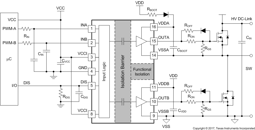
The UCC21220 and UCC21220A devices are basic and functional isolated dual-channel gate drivers with 4A peak-source and 6A peak-sink current. They are designed to drive power MOSFETs and GaNFETs in PFC, Isolated DC/DC, and synchronous rectification applications, with fast switching performance and robust ground bounce protection through greater than 125V/ns common-mode transient immunity (CMTI).
These devices can be configured as two low-side drivers, two high-side drivers, or half-bridge drivers. Two outputs can be paralleled to form a single driver which doubles the drive strength for heavy load conditions due to the best-in-class delay matching performance.
Protection features include the following: DIS pin shuts down both outputs simultaneously when it is set high, all supplies have undervoltage lockout (UVLO), and active pulldown protection clamps the output below 2V when unpowered or floated.
With these features, these devices enable high efficiency, high power density, and robustness in a wide variety of power applications.
 Typical Application