SN65HVD01 3.3V RS-485 with Flexible I/O Supply and Selectable Speed
1 Features
- Exceeds Requirements of TIA-485 Standard
- 1.65-V to 3.6-V Supply for Data and Enable Signals
- 3-V to 3.6-V Supply for Bus Signals
- SLR Pin Selectable Data Rates: 250 kbps or 20 Mbps
- 1/8th Unit Load to Support up to 256 Nodes on a Bus
- Small 3 mm x 3 mm SON Package
- Failsafe Receiver (Bus Open, Bus Shorted, Bus Idle)
- Operating Temperature Range: –40°C to 125°C
- Bus-Pin Protection More Than:
3 Description
The SN65HVD01 is a low-power, 250 kbps or 20 Mbps data rate selectable RS-485 transceiver, utilizing a 1.65-V to 3.6-V supply for data and enable signals, and a 3.3 V ± 10% supply for bus signals. The device is designed for applications requiring synchronous (parallel transceiver) signal timing. On-chip transient suppression protects the device against destructive IEC 61000 ESD and EFT transients.
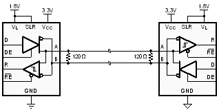
The device combines a differential driver and a differential receiver, connected internally to form a bus port suitable for half-duplex (two-wire bus) communication. The device features a wide common-mode voltage range making it suitable for multi-point applications over long cable runs. The SN65HVD01 is available in a tiny, 3 mm x 3 mm, SON package with operation characterized from -40°C to 125°C.
4 Revision History
Changes from E Revision (March 2014) to F Revision
- Changed Figure 22 image and CH3 scale from: 100 V/div To 2 V/divGo
- Changed Figure 23 CH3 scale from: 100 V/div To 2 V/divGo
Changes from D Revision (November 2013) to E Revision
- Changed the data sheet to the new TI standard layout Go
- Added the Device Information Table Go
- Added the Handling Ratings tableGo
- Added the Detailed Description sectionGo
- Changed Figure 17Go
- Added the Applications and Implementation sectionGo
- Deleted the Application Information sectionGo
- Added the Power Supply RecommendationsGo
- Added the Layout section Go
Changes from C Revision (November 2013) to D Revision
- Changed Feature From: Small 3 mm x 3 mm VQFN Package To: Small 3 mm x 3 mm SON PackageGo
- Changed Feature From: Bus-Pin Protection: To: Bus-Pin Protection More Than: Go
- Changed Feature From: ≤ 15kV To: ±15 kV HBM ProtectionGo
- Changed Feature From: ≤ 15kV To: ±16 kV Contact DischargeGo
- Changed Feature From: ≤ 15kV To: ±16 kV Air DischargeGo
- Changed DESCRIPTION text From: 3 mm x 3 mm, VQFN package To: 3 mm x 3 mm, SON packageGo
- Changed the ABSOLUTE MAXIMUM RATINGS for IEC 61000-4-2 ESD (Air-Gap Discharge) From MAX = ±15 To: MAX = ±16Go
- Changed the ABSOLUTE MAXIMUM RATINGS for IEC 61000-4-2 ESD (Contact Discharge) From MAX = ±15 To: MAX = ±16Go
- Changed the Thermal Information table package From VQFN (DRC) To; SON (DRC)Go
Changes from B Revision (October 2013) to C Revision
- Changed from Product Preview to Production DataGo
Changes from A Revision (October 2013) to B Revision
- Added 8 Typical Characteristics curvesGo
Changes from * Revision (July 2013) to A Revision
- Changed Feature From: 1.8-V to 3.3-V Supply for Data and Enable Signals To: 1.65-V to 3.6-V Supply for Data and Enable SignalsGo
- Changed Feature From: 3.3 V Supply for Bus Signals To: 3-V to 3.6-V Supply for Bus SignalsGo
- Changed Feature From: Selectable Data Rates: 250 kbps or 20 Mbps To: SLR Pin Selectable Data Rates: 250 kbps or 20 MbpsGo
- Changed the list of APPLICATIONSGo
- Changed the DESCRIPTIONGo
- Changed From: 100 Ω resistors To: 120 Ω resistors in the Typical Application circuitGo
- Changed the ELECTRICAL CHARACTERISTICS table valuesGo
- Changed the SWITCHING CHARACTERISTICS table valuesGo
- Changed VCC and 3 V to VL in Figure 9 through Figure 16Go
- Changed Figure 17Go
5 Pin Configuration and Functions
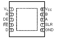
Pin Functions
| NAME | NO. | I/O | DESCRIPTION |
|---|---|---|---|
| VL | 1 | Logic Supply | 1.65 V to 3.6 V supply for logic I/O signals R, RE, D, DE, and SLR) |
| R | 2 | Digital Output | Receive data output |
| DE | 3 | Digital Input | Driver enable input |
| RE | 4 | Digital Input | Receiver enable input |
| D | 5 | Digital Input | Transmission data input |
| GND | 6 | Reference Potential | Local device ground |
| SLR | 7 | Digital Input | Slew rate select: Low = 20 Mbps, High = 250 kbps. Defaults to 20 Mbps if SLR is left floating |
| A | 8 | Bus I/O | Digital bus I/O, A |
| B | 9 | Bus I/O | Digital bus I/O, B |
| VCC | 10 | Bus Supply | 3 V to 3.6 V supply for A and B bus lines |
6 Specifications
6.1 Absolute Maximum Ratings(1)
| VALUE | UNIT | ||
|---|---|---|---|
| MIN | MAX | ||
| Control supply voltage, VL | –0.5 | 4 | V |
| Bus supply voltage, VCC | –0.5 | 5.5 | V |
| Voltage range at A or B Inputs | –13 | 16.5 | V |
| Input voltage range at any logic terminal | –0.3 | 5.7 | V |
| Voltage input range, transient pulse, A and B, through 100Ω | –100 | 100 | V |
| Receiver output current | –12 | 12 | mA |
| Junction temperature, TJ | 170 | °C | |
| Continuous total power dissipation | See the Thermal Information table | ||
Handling Ratings
| MIN | MAX | UNIT | ||
|---|---|---|---|---|
| TSTG | Storage temperature range | –65 | 150 | °C |
| VESD | IEC 60749-26 ESD (Human Body Model), bus terminals and GND | ±15 | kV | |
| IEC 61000-4-2 ESD (Air-Gap Discharge), bus terminals and GND (1) | ±16 | kV | ||
| IEC 61000-4-2 ESD (Contact Discharge), bus terminals and GND | ±16 | kV | ||
| IEC 61000-4-4 EFT (Fast transient or burst) bus terminals and GND | ±4 | kV | ||
| JEDEC Standard 22, Test Method A114 (Human Body Model), all terminals | ±8 | kV | ||
| JEDEC Standard 22, Test Method C101 (Charged Device Model), all terminals | ±1.5 | kV |
6.2 Recommended Operating Conditions
| MIN | NOM | MAX | UNIT | |||
|---|---|---|---|---|---|---|
| VL | Control supply voltage | 1.65 | 3.6 | V | ||
| VCC | Bus supply voltage | 3 | 3.3 | 3.6 | V | |
| VI | Input voltage at any bus terminal (separately or common mode) (1) | –7 | 12 | V | ||
| VIH | High-level input voltage (Driver, driver enable, receiver enable inputs, and slew rate select) | 0.7×VL | VL | V | ||
| VIL | Low-level input voltage (Driver, driver enable, receiver enable inputs, and slew rate select) | 0 | 0.3×VL | V | ||
| VID | Differential input voltage | –12 | 12 | V | ||
| IO | Output current | Driver | –80 | 80 | mA | |
| Receiver | –2 | 2 | mA | |||
| RL | Differential load resistance | 54 | 60 | Ω | ||
| CL | Differential load capacitance | 50 | pF | |||
| 1/tUI | Signaling rate | SLR = '0' | 20 | Mbps | ||
| SLR = '1' | 250 | kbps | ||||
| TA(2) | Operating free-air temperature Thermal Information | –40 | 125 | °C | ||
6.3 Thermal Information
| PARAMETER(1) | SON (DRC) | UNIT | |
|---|---|---|---|
| ΘJA | Junction-to-Ambient Thermal Resistance | 41.4 | °C/ W |
| ΘJC(top) | Junction-to-Case(top) Thermal Resistance | 48.7 | |
| ΘJB | Junction-to-Board Thermal Resistance | 18.8 | |
| ΨJT | Junction-to-Top characterization parameter | 0.6 | |
| ΨJB | Junction-to-Board characterization parameter | 19 | |
| ΘJC(bottom) | Junction-to-Case(bottom) Thermal Resistance | 3.7 | |
| TTSD | Thermal Shut-down junction temperature | 170 | °C |
6.4 Dissipation Ratings
| PARAMETER | TEST CONDITIONS | VALUE | UNIT | |||
|---|---|---|---|---|---|---|
| PD | Power Dissipation driver and receiver enabled, VCC = VL = 3.6 V, TJ = 150°C, 50% duty cycle square-wave signal at signaling rate |
Unterminated | RL = 300 Ω, CL = 50 pF (driver) |
250 kbps | 125 | mW |
| 20 Mbps | 175 | |||||
| RS-422 load | RL = 100 Ω, CL = 50 pF (driver) |
250 kbps | 165 | mW | ||
| 20 Mbps | 215 | |||||
| RS-485 load | RL = 54 Ω, CL = 50 pF (driver) |
250 kbps | 200 | mW | ||
| 20 Mbps | 250 | |||||
6.5 Electrical Characteristics
over recommended operating range (unless otherwise specified)| PARAMETER | TEST CONDITIONS | MIN | TYP | MAX | UNIT | |||
|---|---|---|---|---|---|---|---|---|
| |VOD| | Driver differential output voltage magnitude | RL = 60 Ω, 375 Ω on each output to –7 V to 12 V |
See Figure 9 | 1.5 | 2 | V | ||
| RL = 54 Ω (RS-485) | See Figure 10 | 1.5 | 2 | V | ||||
| RL = 100 Ω (RS-422) TJ ≥ 0°C, VCC ≥ 3.2V |
2 | V | ||||||
| Δ|VOD| | Change in magnitude of driver differential output voltage | RL = 54 Ω, CL = 50 pF | –50 | 0 | 50 | mV | ||
| VOC(SS) | Steady-state common-mode output voltage | Center of two 27-Ω load resistors | 1 | VCC/2 | 3 | V | ||
| ΔVOC | Change in differential driver output common-mode voltage | –50 | 0 | 50 | mV | |||
| VOC(PP) | Peak-to-peak driver common-mode output voltage | 500 | mV | |||||
| COD | Differential output capacitance | 15 | pF | |||||
| VIT+ | Positive-going receiver differential input voltage threshold | See (1) | –60 | –20 | mV | |||
| VIT– | Negative-going receiver differential input voltage threshold | –200 | –130 | See (1) | mV | |||
| VHYS | Receiver differential input voltage threshold hysteresis (VIT+ – VIT–) |
40 | 70 | mV | ||||
| VOH | Receiver high-level output voltage | VL = 1.65 V, IOH = -2 mA | 1.3 | 1.45 | V | |||
| VL = 3 V, IOH = -2 mA | 2.8 | 2.9 | ||||||
| VOL | Receiver low-level output voltage | VL = 1.65 V, IOL = 2 mA | 0.2 | 0.35 | V | |||
| VL = 3 V, IOL = 2 mA | 0.1 | 0.2 | ||||||
| II | Driver input, driver enable, and receiver enable input current | –2 | 2 | µA | ||||
| IOZ | Receiver output high-impedance current | VO = 0 V or VL, RE at VL | –1 | 1 | µA | |||
| IOS | Driver short-circuit output current | –150 | 150 | mA | ||||
| II | Bus input current (disabled driver) | VL = 1.8 V, VCC = 3.3 V, DE at 0 V |
VI = 12 V | 85 | 125 | µA | ||
| VI = –7 V | –100 | –60 | µA | |||||
| ICC | Supply current (quiescent) | Driver and Receiver enabled | DE=VL, RE = GND, No load | 750 | 1100 | µA | ||
| TJ ≤ 85°C | 1000 | µA | ||||||
| Driver enabled, receiver disabled | DE=VCC, RE = VL, No load | 350 | 650 | µA | ||||
| Driver disabled, receiver enabled | DE=GND, RE = GND, No load | 650 | 800 | µA | ||||
| Driver and receiver disabled | DE=GND, RE = VL, No load | 0.1 | 5 | µA | ||||
| Supply current (dynamic) | See the Typical Characteristics section | |||||||
6.6 Switching Characteristics
over recommended operating conditions| PARAMETER | TEST CONDITIONS | MIN | TYP | MAX | UNIT | ||
|---|---|---|---|---|---|---|---|
| DRIVER, SLR = '1', 250 kbps, bit time ≥ 4 µs | |||||||
| tr, tf | Driver differential output rise/fall time | RL = 54 Ω, CL = 50 pF | See Figure 11 | 0.4 | 0.8 | 1.2 | µs |
| tPHL, tPLH | Driver propagation delay | 0.4 | 0.8 | 1.2 | µs | ||
| tSK(P) | Driver pulse skew, |tPHL – tPLH| | 0.2 | µs | ||||
| tPHZ, tPLZ | Driver disable time | See Figure 12 and Figure 13 | 0.025 | 0.1 | µs | ||
| tPZH, tPZL | Driver enable time | Receiver enabled | 0.6 | 1 | µs | ||
| Receiver disabled | 3.5 | 8 | µs | ||||
| DRIVER, SLR = '0', 20 Mbps, bit time ≥ 50 ns | |||||||
| tr, tf | Driver differential output rise/fall time | RL = 54 Ω, CL = 50 pF |
See Figure 11 | 5 | 10 | 15 | ns |
| tPHL, tPLH | Driver propagation delay | 6 | 15 | 25 | ns | ||
| tSK(P) | Driver pulse skew, |tPHL – tPLH| | 4 | ns | ||||
| tPHZ, tPLZ | Driver disable time | See Figure 12 and Figure 13 | 20 | 35 | ns | ||
| tPZH, tPZL | Driver enable time | Receiver enabled | 14 | 30 | ns | ||
| Receiver disabled | 3 | 7 | µs | ||||
| RECEIVER, SLR = 'X' | |||||||
| tr, tf | Receiver output rise/fall time | CL = 15 pF | See Figure 14 | 5 | 15 | ns | |
| tPHL, tPLH | Receiver propagation delay time | 30 | 60 | 90 | ns | ||
| tSK(P) | Receiver pulse skew, |tPHL – tPLH| | 15 | ns | ||||
| tPLZ, tPHZ | Receiver disable time | 10 | 20 | ns | |||
| tpZL(1), tPZH(1)
tPZL(2), tPZH(2) |
Receiver enable time | Driver enabled | See Figure 15 | 15 | 80 | ns | |
| Driver disabled | See Figure 16 | 3 | 8 | µs | |||
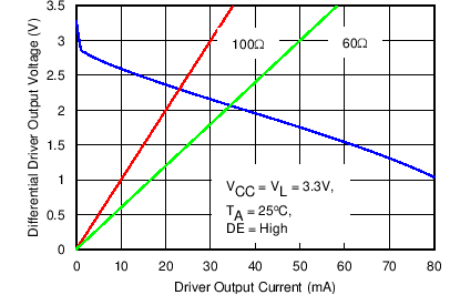
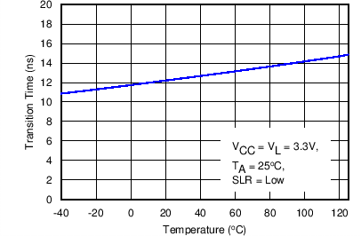
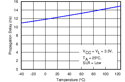
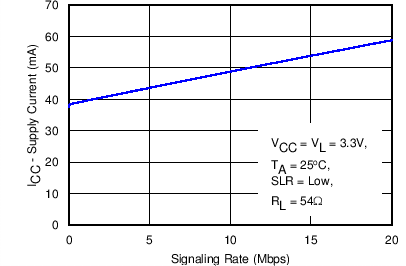
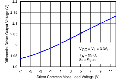
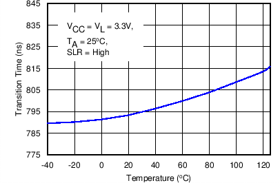
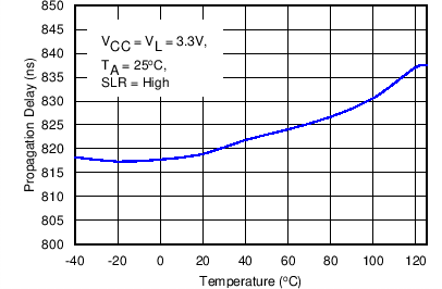
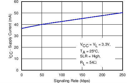
6.7 Typical Characteristics