-
BQ24392 Dual SPST USB 2.0 High Speed Switch with USB Battery Charging Specification Revision 1.2 Detection
- 1 Features
- 2 Applications
- 3 Description
- 4 Revision History
- 5 Pin Configuration and Functions
- 6 Specifications
- 7 Detailed Description
- 8 Application and Implementation
- 9 Power Supply Recommendations
- 10Layout
- 11Device and Documentation Support
- 12Mechanical, Packaging, and Orderable Information
- IMPORTANT NOTICE
BQ24392 Dual SPST USB 2.0 High Speed Switch with USB Battery Charging Specification Revision 1.2 Detection
1 Features
- USB 2.0 High Speed Switch
- Detects USB Battery Charging Specification Version 1.2 (BCv1.2) Compliant Chargers
- Compatible Accessories
- Dedicated Charging Port
- Standard Downstream Port
- Charging Downstream Port
- Non-Standard Chargers
- Apple™ Charger
- TomTom™ Charger
- USB Chargers Not Compliant With Battery Charging Specification Version 1.2 (BCv1.2)
- –2 V to 28 V VBUS Voltage Range
- ESD Performance Tested per JESD 22
- 4000-V Human-Body Model
- 1500-V Charged-Device Model (C101)
- ESD Performance DP_CON/DM_CON to GND
- ±8-kV Contact Discharge (IEC 61000-4-2)
2 Applications
- Mobile Phones
- Smart Phones
- Cameras
- GPS Systems
3 Description
The BQ24392 is a dual single-pole single-throw (SPST) USB 2.0 high-speed isolation switch with charger detection capabilities for use with micro and mini-USB ports. This USB switch allows mobile phones, tablets, and other battery operated electronics to be charged from different adapters with minimal system software. The device’s charger detection circuitry can support USB Battery Charging Specification version 1.2 (BCv1.2) compliant, Apple™, TomTom™, and other non-standard chargers.
The BQ24392 device is powered through VBUS when a charger is attached to the micro or mini-USB port and has a 28-V tolerance to avoid the need for external protection.
Device Information(1)
| PART NUMBER | PACKAGE | BODY SIZE (NOM) |
|---|---|---|
| BQ24392 | UQFN (10) | 2.05 mm × 1.55 mm |
- For all available packages, see the orderable addendum at the end of the datasheet.
SPACER
SPACER
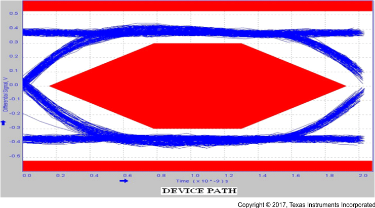
480-Mbps USB 2.0 Eye Diagram With USB Switch

4 Revision History
Changes from F Revision (July 2017) to G Revision
- Changed RON From: 8 Ω TYP To: 3.5 Ω TYP, 6.9 Ω MAX in the Electrical Characteristic table Go
Changes from E Revision (February 2017) to F Revision
- Changed CHG_DET diode direction from right facing to left facing in Application Schematic. Go
Changes from D Revision (January 2016) to E Revision
- Changed From: BQ24932 To: BQ24392 in the DescriptionGo
- Changed From: BQ24932 To: BQ24392 in the OverviewGo
- Changed title From: Using the BQ24932 GPIOs To: Using the BQ24392 GPIOsGo
Changes from C Revision (January 2015) to D Revision
- Changed diode direction from left facing to right facing in Application Schematic. Go
Changes from B Revision (October 2014) to C Revision
- Updated Features. Go
Changes from A Revision (June 2012) to B Revision
- Added ESD Rating table, Feature Description section, Device Functional Modes, Application and Implementation section, Power Supply Recommendations section, Layout section, Device and Documentation Support section, and Mechanical, Packaging, and Orderable Information section. Go
5 Pin Configuration and Functions

Pin Functions
| PIN | I/O | DESCRIPTION | |
|---|---|---|---|
| NO. | NAME | ||
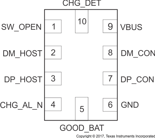
| 1 | SW_OPEN | O | USB switch status indicator Open-drain output. 10kΩ external pull-up resistor required SW_OPEN = LOW indicates when switch is connected SW_OPEN = HIGH-Z indicates when then switch is not connected |
| 2 | DM_HOST | I/O | D– signal to transceiver |
| 3 | DP_HOST | I/O | D+ signal to transceiver |
| 4 | CHG_AL_N | O | Charging status indicator Open-drain output. 10kΩ external pull-up resistor required CHG_AL_N = LOW indicates when charging is allowed CHG_AL_N = HIGH-Z indicates when charging is not allowed |
| 5 | GOOD_BAT | I | Battery status indication from system GOOD_BAT = LOW indicates a dead battery GOOD_BAT = HIGH indicates a good battery |
| 6 | GND | - | Ground |
| 7 | DP_CON | I/O | D+ signal from USB connector |
| 8 | DM_CON | I/O | D– signal from USB connector |
| 9 | VBUS | I | Supply pin from USB connector |
| 10 | CHG_DET | O | Charger detection indicator Push-Pull output to system CHG_DET = LOW indicates when a charger is not detected CHG_DET = HIGH indicates when a charger detected |
6 Specifications
6.1 Absolute Maximum Ratings
over –40℃ to 85℃ temperature range (unless otherwise noted)| MIN | MAX | UNIT | ||
|---|---|---|---|---|
| Input Voltage | VBUS | –2 | 28 | V |
| CHG_AL_N | –2 | 28 | V | |
| DM_HOST | –0.3 | 7 | V | |
| DP_HOST | –0.3 | 7 | ||
| GOOD_BAT | –0.3 | 7 | ||
| DP_CON | –0.3 | 7 | ||
| DM_CON | –0.3 | 7 | ||
| CHG_DET | –0.3 | 7 | ||
| Tstg | Storage temperature range | 65 | 150 | °C |
6.2 ESD Ratings
| VALUE | UNIT | |||
|---|---|---|---|---|
| V(ESD) | Electrostatic discharge | Human-body model (HBM), per ANSI/ESDA/JEDEC JS-001(1) | ±4000 | V |
| Charged-device model (CDM), per JEDEC specification JESD22-C101(2) | ±1500 | |||
| IEC Contact discharge pins DP_CON and DM_CON to GND | ±8000 | |||
6.3 Recommended Operating Conditions
| MIN | MAX | UNIT | ||
|---|---|---|---|---|
| VBUS | 4.75 | 5.25 | V | |
| GOOD_BAT | 0 | VBUS | ||
| DM_HOST | 0 | 3.6 | ||
| DP_HOST | 0 | 3.6 | ||
| DM_CON | 0 | 3.6 | ||
| DP_CON | 0 | 3.6 | ||
6.4 Thermal Information
| THERMAL METRIC(1) | bq24392 | UNIT | |
|---|---|---|---|
| RSE | |||
| 10 PINS | |||
| RθJA | Junction-to-ambient thermal resistance | 167.7 | °C/W |
| RθJC(top) | Junction-to-case (top) thermal resistance | 78.8 | °C/W |
| RθJB | Junction-to-board thermal resistance | 95.8 | °C/W |
| ψJT | Junction-to-top characterization parameter | 4.7 | °C/W |
| ψJB | Junction-to-board characterization parameter | 95.9 | °C/W |
6.5 Electrical Characteristics
VBUS = 4.5 V to 5.5 V, TA = –40°C to 85°C (unless otherwise noted)(1)6.6 Typical Characteristics


7 Detailed Description
7.1 Overview
The BQ24392 is a USB 2.0 high-speed isolation switch with charger detection capabilities for use with micro and mini-USB ports. Upon plugin of a Battery Charging Specification 1.2 (BCv1.2) compliant, Apple™, TomTom™, or other USB charger into a micro or mini-USB connector, the device will automatically detect the charger and operate the USB 2.0 high-speed isolation switch.
The BQ24392 device is powered through VBUS when a charger is attached to the micro or mini-USB port and has a 28-V tolerance to avoid the need for external protection.
7.2 Functional Block Diagram

7.3 Feature Description
7.3.1 Charger Detection
 Figure 3. Charge Detection Block Diagram
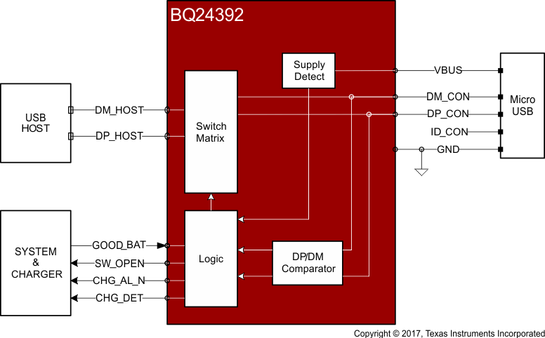
When a micro or mini-USB accessory is inserted into the connector and once VBUS is greater than VVBUS_VALID threshold, the BQ24392 will enter into the Data Contact Detection (DCD) state which includes a 600-ms timeout feature that is prescribed in the USB Battery Charging Specification version 1.2 (BCv1.2). If the micro or mini-USB accessory is determined to be USB BCv1.2 compliant, a 130-ms debounce period will initiate and the BQ24392 will proceed to its primary detection and then secondary detection states to determine if a Dedicated Charging Port (DCP), Standard Downstream Port (SDP), or Charging Downstream Port (CDP) is attached to the USB-port. The minimum detection time for a DCP, SDP, and CDP is 130 ms, but can be as long as 600 ms due to the slow plug in effect.
If the GOOD_BAT pin is high, the USB 2.0 switches are automatically closed to enable data transfer after the device detects a Standard Downstream Port (SDP) or Charging Downstream Port (CDP) was connected.
If Data Contact Detection (DCD) fails, the BQ24392 proceeds to detect whether an Apple or TomTom charger was inserted by checking the voltage level on DP_CON and DM_CON. Thus, for Apple and TomTom chargers, detection time typically takes ~600 ms.
The 3 output pins CHG_AL_N, CHG_DET, and SW_OPEN change their status at the end of detection. Table 1 is the detection table with the GPIO status for each type of supported charger. More information on how to use the GPIOs is available in Using the BQ24392 GPIOs .
Table 1. Detection Table
| Device Type | VBUS | DP_CON (D+) |
DM_CON (D–) |
GOOD_BAT (Input) |
CHG_AL_N (Output) |
CHG_DET (Output) |
SW_OPEN (Output) |
Switch Status | Charge Current |
|---|---|---|---|---|---|---|---|---|---|
| Standard Downstream Port |
> 3.5 V | Pull-down R to GND | Pull-down R to GND | HIGH | LOW | LOW | LOW | Connected | Charge with 100 mA/ Change the input current based on enumeration |
| LOW | LOW | LOW | High-Z | Not Connected | Charge with 100 mA | ||||
| Charging Downstream Port |
> 3.5 V | Pull-down R to GND | VDM_SRC | HIGH | LOW | HIGH | LOW | Connected | Charge with full current |
| LOW | LOW | HIGH | High-Z | Not Connected | Charge with 100 mA | ||||
| Dedicated Charging Port |
> 3.5 V | Short to D– | Short to D+ | X | LOW | HIGH | High-Z | Not Connected | Charge with full current |
| Apple Charger | > 3.5 V | 2.0 < VDP_CON < 2.8 | 2.0 < VDM_CON < 2.8 | X | LOW | HIGH | High-Z | Not Connected | Charge with full current |
| TomTom Charger | > 3.5 V | 2.0 < VDP_CON < 3.1 | 2.0 < VDM_CON < 3.1 | X | LOW | HIGH | High-Z | Not Connected | Charge with full current |
| PS/2 Charger | > 3.5 V | Pull-up R to VVBUS | Pull-up R to VVBUS | X | LOW | LOW | High-Z | Not Connected | Charge with 100 mA |
| Non-compliant USB Charger |
> 3.5 V | Open | Open | X | LOW | LOW | High-Z | Not Connected | Charge with 100 mA |
| Any Device | < 3.5 V | Open | Open | X | High-Z | LOW | High-Z | Not Connected | No Charge |
| Any Device DBP Timer Expired |
> 3.5 V | X | X | LOW | High-Z | LOW | High-Z | Not Connected | No Charge |
If a charge has been detected and the GOOD_BAT pin is low, a Dead Battery Provision (DBP) timer is initiated. If the GOOD_BAT continues to be low for 30 minutes (maximum of 45 minutes), charging is disabled and CHG_AL_N goes into the High-Z state to indicate this. Toggling GOOD_BAT high after the DBP timer expires re-starts detection and the DBP timer.
7.4 Device Functional Modes
The BQ24392 has two functional modes USB switch ON and USB switch OFF.