-
PCM514x 2-VRMS DirectPath™, 112/106-dB Audio Stereo DAC With 32-bit, 384-kHz PCM Interface
- 1 Features
- 2 Applications
- 3 Description
- 4 Revision History
- 5 Device Comparison
- 6 Pin Configuration and Functions
-
7 Specifications
- 7.1 Absolute Maximum Ratings
- 7.2 ESD Ratings
- 7.3 Recommended Operating Conditions
- 7.4 Thermal Information
- 7.5 Electrical Characteristics
- 7.6 Timing Requirements: SCK Input
- 7.7 Timing Requirements: PCM Audio Data
- 7.8 Timing Requirements: XSMT
- 7.9 Switching Characteristics
- 7.10 Typical Characteristics
-
8 Detailed Description
- 8.1 Overview
- 8.2 Functional Block Diagram
- 8.3
Feature Description
- 8.3.1 Terminology
- 8.3.2 Audio Data Interface
- 8.3.3 XSMT Pin (Soft Mute / Soft Un-Mute)
- 8.3.4 Audio Processing
- 8.3.5 DAC Outputs
- 8.3.6
Reset and System Clock Functions
- 8.3.6.1 Clocking Overview
- 8.3.6.2 Clock Slave Mode With Master and System Clock (SCK) Input (4 Wire I2S)
- 8.3.6.3 Clock Slave Mode With BCK PLL to Generate Internal Clocks (3-Wire PCM)
- 8.3.6.4 Clock Generation Using the PLL
- 8.3.6.5 PLL Calculation
- 8.3.6.6 Clock Master Mode from Audio Rate Master Clock
- 8.3.6.7 Clock Master from a Non-Audio Rate Master Clock
- 8.4 Device Functional Modes
- 8.5 Programming
- 9 Application and Implementation
- 10Power Supply Recommendations
- 11Layout
- 12Register Maps
- 13Device and Documentation Support
- 14Mechanical, Packaging, and Orderable Information
- IMPORTANT NOTICE
PCM514x 2-VRMS DirectPath™, 112/106-dB Audio Stereo DAC With 32-bit, 384-kHz PCM Interface
1 Features
- Programmable miniDSP
- Market-Leading Low Out-of-Band Noise
- Selectable Digital-Filter Latency and Performance
- No DC Blocking Capacitors Required
- Integrated Negative Charge Pump
- Intelligent Muting System; Soft Up or Down Ramp and Analog Mute For 120-dB Mute SNR
- Integrated High-Performance Audio PLL With BCK Reference To Generate SCK Internally
- Accepts 16-, 20-, 24-, And 32-Bit Audio Data
- PCM Data Formats: I2S, Left-Justified, Right-Justified, TDM / DSP
- SPI or I2C Control
- Software or Hardware Configuration
- Automatic Power-Save Mode When LRCK And BCK Are Deactivated
- 1.8-V or 3.3-V Fail-Safe LVCMOS Digital Inputs
- Single Supply Operation:
3.3-V Analog, 1.8-V or 3.3-V Digital - Integrated Power-On Reset
- Small 28-pin TSSOP Package
2 Applications
- A/V Receivers
- DVD, BD Players
- HDTV Receivers
- Applications Requiring 2-VRMS Audio Output
3 Description
The PCM514x devices are a family of monolithic CMOS-integrated circuits that include a stereo digital-to-analog converter and additional support circuitry in a small TSSOP package. The PCM514x uses the latest generation of TI’s advanced segment-DAC architecture to achieve excellent dynamic performance and improved tolerance to clock jitter.
Members of the PCM514x family integrate a fully programmable miniDSP core, allowing developers to integrate filters, dynamic range controls, custom interpolators, and other differentiating features to their products.
The PCM514x provides 2.1-VRMS ground centered outputs, allowing designers to eliminate DC-blocking capacitors on the output, as well as external muting circuits traditionally associated with single-supply line drivers.
The integrated line driver surpasses all other charge-pump-based line drivers by supporting loads down to 1 kΩ, allowing the PCM514x to drive up to 10 products in parallel, such as LCD TV, DVDR, and AV receivers.
The integrated PLL on the device removes the requirement for a system clock (commonly known as master clock), allowing a 3-wire I2S connection and reducing system EMI.
Device Information
| DEVICE NAME | PACKAGE | BODY SIZE (NOM) |
|---|---|---|
| PCM5141 | TSSOP (28) | 9.70 mm × 4.40 mm |
| PCM5142 |
.
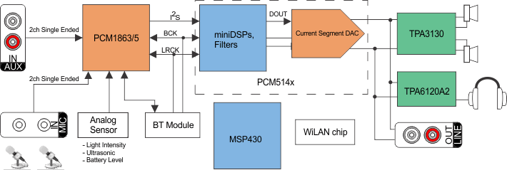
Simplified System Diagram
4 Revision History
Changes from A Revision (September 2012) to B Revision
- Deleted Internal Pop-Free Control For Sample-Rate Changes Or Clock Halts, ... With Popless OperationGo
- Changed Accepts 16-, 24-, And 32-Bit Audio Data to Accepts 16-, 20-, 24-, And 32-Bit Audio DataGo
- Added Pin Configuration and Functions section, ESD Ratings table, Feature Description section, Device Functional Modes, Application and Implementation section, Power Supply Recommendations section, Layout section, Device and Documentation Support section, and Mechanical, Packaging, and Orderable Information sectionGo
- Clarified Pin Functions table.Go
- Changed Operating temperature to Operating junction temperature in Absolute Maximum RatingsGo
- Deleted redundant PLL specification in Recommended Operating Conditions Go
- Deleted Intelligent clock error... and ...for pop-free performance in the Overview section.Go
- Added note on instruction cycles to PCM512x Audio Processing.Go
- Deleted text The Graphical Development Environment consists of number of Hybrid Flows that can be downloaded to the device and run on the miniDSP. From: Software Go
- Added note on instruction cycles in Fixed Audio Processing Flow (Program 5).Go
- Changed Ouptut to OutputGo
- Deleted VREF mode provides 2.1Vrms full-scale output at both AVDD levels.Go
- Clarified clock generation explanation in Reset and System Clock FunctionsGo
- Clarified external SCK discussion in Clock Slave Mode with BCK PLL to Generate Internal Clocks (3-Wire PCM).Go
- Deleted The PCM514x disables the internal PLL when an external SCK is supplied.Go
5 Device Comparison
Table 1. Differences Between PCM514x Devices
| PART NUMBER | DYNAMIC RANGE | SNR | THD |
|---|---|---|---|
| PCM5142A | 112 dB | 112 dB | –93 dB |
| PCM5141A | 106 dB | 106 dB | –92 dB |
Table 2. Typical Performance (3.3-V Power Supply)
| PARAMETER | PCM5142 / PCM5141 |
|---|---|
| SNR | 112 / 106 dB |
| Dynamic range | 112 /106 dB |
| THD+N at –1 dBFS | –93/ –92 dB |
| Full-scale single-ended output | 2.1 VRMS (GND center) |
| Normal 8× oversampling digital filter latency | 20tS |
| Low latency 8× oversampling digital filter latency | 3.5tS |
| Sampling frequency | 8 kHz to 384 kHz |
| System clock multiples (fSCK): 64, 128, 192, 256, 384, 512, 768, 1024, 1152, 1536, 2048, 3072 | Up to 50 MHz |
6 Pin Configuration and Functions
RHB Package
I2C Mode
(MODE1 tied to DGND and MODE2 tied to DVDD)
Top View

RHB Package
Hardwired Mode
(MODE1 tied to DGND, MODE2 tied to DGND)
Top View
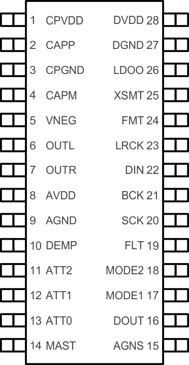
RHB Package
SPI Mode
(MODE1 tied to DVDD)
Top View

Table 3. Gain and Attenuation in Hardwired Mode
| ATT PIN CONDITION (ATT2 : ATT1 : ATT0) | GAIN AND ATTENUATION LEVEL |
|---|---|
| ( 0 0 0 ) | 0 dB |
| ( 0 0 1 ) | 3 dB |
| ( 0 1 0 ) | 6 dB |
| ( 0 1 1 ) | 9 dB |
| ( 1 0 0 ) | 12 dB |
| ( 1 0 1 ) | 15 dB |
| ( 1 1 0 ) | –6 dB |
| ( 1 1 1 ) | –3 dB |
6.1 Pin Functions
| PIN | I/O | DESCRIPTION | |||||
|---|---|---|---|---|---|---|---|
| NAME | MODE, NO. | ||||||
| I2C | SPI | HW | |||||
| CPVDD | 1 | 1 | 1 | - | Charge pump power supply, 3.3 V | ||
| CAPP | 2 | 2 | 2 | O | Charge pump flying capacitor terminal for positive rail | ||
| CPGND | 3 | 3 | 3 | - | Charge pump ground | ||
| CAPM | 4 | 4 | 4 | O | Charge pump flying capacitor terminal for negative rail | ||
| VNEG | 5 | 5 | 5 | O | Negative charge pump rail terminal for decoupling, –3.3 V | ||
| OUTL | 6 | 6 | 6 | O | Analog output from DAC left channel | ||
| OUTR | 7 | 7 | 7 | O | Analog output from DAC right channel | ||
| AVDD | 8 | 8 | 8 | - | Analog power supply, 3.3 V | ||
| AGND | 9 | 9 | 9 | - | Analog ground | ||
| VCOM | 10 | 10 | – | O | I2C, SPI | VCOM output (optional mode selected by register; default setting is VREF mode.) When in VREF mode (default), this pin ties to GND. When in VCOM mode, decoupling capacitor to GND is required. | |
| DEMP | – | – | 10 | I | HW | DEMP: De-emphasis control for 44.1-kHz sampling rate: Off (Low) / On (High) | |
| SDA | 11 | – | – | I/O | I2C | Data for I2C(1)(2) | |
| MOSI | – | 11 | – | I | SPI | Input data for SPI(2) | |
| ATT2 | – | – | 11 | HW | Digital gain and attenuation control pin | ||
| SCL | 12 | – | – | I | I2C | Input clock for I2C(2) | |
| MC | – | 12 | – | SPI | Input clock for SPI(2) | ||
| ATT1 | – | – | 12 | HW | Digital gain and attenuation control pin | ||
| GPIO5 | 13 | 13 | – | I/O | I2C, SPI | General purpose digital input and output port (3) | |
| ATT0 | – | – | 13 | HW | Digital gain and attenuation control pin | ||
| GPIO4 | 14 | 14 | – | I/O | I2C, SPI | General purpose digital input and output port (3) | |
| MAST | – | – | 14 | HW | I2S Master clock select pin : Master (High) BCK/LRCK outputs, Slave (Low) BCK/LRCK inputs | ||
| GPIO3 | 15 | 15 | – | I/O | I2C, SPI | General purpose digital input and output port (3) | |
| AGNS | – | – | 15 | HW | Analog gain selector : 0-dB 2-VRMS output (Low), –6-dB 1-VRMS output (High) | ||
| ADR2 | 16 | – | – | I/O | I2C | 2nd LSB address select bit for I2C | |
| GPIO2 | – | 16 | – | SPI | General purpose digital input and output port | ||
| DOUT | – | – | 16 | O | HW | General Purpose Output (Low level) | |
| MODE1 | 17 | 17 | 17 | I | Mode control selection pin (2)
MODE1 = Low, MODE2 = Low : Hardwired mode MODE1 = Low, MODE2 = High: I2C mode MODE1 = High: SPI mode |
||
| MODE2 | 18 | – | 18 | I2C, HW | MODE2 | ||
| MS | – | 18 | – | I | SPI | MS pin (chip select for SPI) | |
| GPIO6 | 19 | 19 | – | I/O | I2C, SPI | General purpose digital input and output port | |
| FLT | – | – | 19 | I | HW | Filter select : Normal latency (Low) / Low latency (High) | |
| SCK | 20 | 20 | 20 | I | System clock input(2) | ||
| BCK | 21 | 21 | 21 | I/O | Audio data bit clock input (slave) or output (master)(2) | ||
| DIN | 22 | 22 | 22 | I | Audio data input(2) | ||
| LRCK | 23 | 23 | 23 | I/O | Audio data word clock input (slave) or output (master)(2) | ||
| ADR1 | 24 | – | – | I/O | I2C | LSB address select bit for I2C | |
| MISO (GPIO1) | – | 24 | – | SPI | Primary output data for SPI readback. Secondary; general purpose digital input/output port controlled by register | ||
| FMT | – | – | 24 | HW | Audio format selection : I2S (Low) / Left justified (High) | ||
| XSMT | 25 | 25 | 25 | I | Soft mute control Soft mute(2) (Low) / soft un-mute (High) | ||
| LDOO | 26 | 26 | 26 | - | Internal logic supply rail terminal for decoupling, 1.8 V | ||
| DGND | 27 | 27 | 27 | - | Digital ground | ||
| DVDD | 28 | 28 | 28 | - | Digital power supply, 3.3 V or 1.8 V | ||
7 Specifications
7.1 Absolute Maximum Ratings
over operating free-air temperature range (unless otherwise noted)| MIN | MAX | UNIT | ||
|---|---|---|---|---|
| Supply voltage | AVDD, CPVDD, DVDD | –0.3 | 3.9 | V |
| LDO with DVDD at 1.8 V | –0.3 | 2.25 | ||
| Digital input voltage | DVDD at 1.8 V | –0.3 | 2.25 | V |
| DVDD at 3.3 V | –0.3 | 3.9 | ||
| Analog input voltage | –0.3 | 3.9 | V | |
| Operating junction temperature, TJ | –40 | 130 | °C | |
| Storage temperature, Tstg | –65 | 150 | °C | |
7.2 ESD Ratings
| VALUE | UNIT | |||
|---|---|---|---|---|
| V(ESD) | Electrostatic discharge | Human-body model (HBM), per ANSI/ESDA/JEDEC JS-001(1) | ±2000 | V |
| Charged-device model (CDM), per JEDEC specification JESD22-C101(2) | ±750 | |||
7.3 Recommended Operating Conditions
| MIN | NOM | MAX | UNIT | ||||
|---|---|---|---|---|---|---|---|
| AVDD | Analog power supply voltage | Referenced to AGND(1) | VCOM mode | 3 | 3.3 | 3.46 | V |
| VREF mode | 3.2 | 3.3 | 3.46 | ||||
| DVDD | Digital power supply voltage | Referenced to DGND(1) | 1.8 V DVDD | 1.65 | 1.8 | 1.95 | V |
| 3.3 V DVDD | 3.1 | 3.3 | 3.46 | ||||
| CPVDD | Charge pump supply voltage | Referenced to CPGND(1) | 3.1 | 3.3 | 3.46 | V | |
| MCLK | Master clock frequency | 50 | MHz | ||||
| LOL, LOR | Stereo line output load resistance | 1 | 10 | kΩ | |||
| CLOUT | Digital output load capacitance | 10 | pF | ||||
| TJ | Operating junction temperature | –40 | 130 | °C | |||
7.4 Thermal Information
| THERMAL METRIC(1) | PCM512x | UNIT | ||
|---|---|---|---|---|
| RHB (TSSOP) | ||||
| 32 PINS | ||||
| RθJA | Junction-to-ambient thermal resistance | 72.2 | °C/W | |
| RθJC(top) | Junction-to-case(top) thermal resistance | 17.5 | °C/W | |
| RθJB | Junction-to-board thermal resistance | 35.0 | °C/W | |
| ψJT | Junction-to-top characterization parameter | 0.4 | °C/W | |
| ψJB | Junction-to-board characterization parameter | 34.5 | °C/W | |
7.5 Electrical Characteristics
TA = 25°C, AVDD = CPVDD = DVDD = 3.3 V, fS = 48 kHz, system clock = 512 fS and 24-bit data (unless otherwise noted).| PARAMETER | TEST CONDITIONS | MIN | TYP | MAX | UNIT | |
|---|---|---|---|---|---|---|
| Resolution | 16 | 24 | 32 | Bits | ||
| DIGITAL INPUT/OUTPUT | ||||||
| Logic Family: 3.3-V LVCMOS Compatible | ||||||
| VIH | Input logic level, high | 0.7 × DVDD | V | |||
| VIL | Input logic level, low | 0.3 × DVDD | V | |||
| IIH | Input logic current, high | VIN = VDD | 10 | µA | ||
| IIL | Input logic current, low | VIN = 0 V | –10 | µA | ||
| VOH | Output logic level, high | IOH = –4 mA | 0.8 × DVDD | V | ||
| VOL | Output logic level, low | IOL = 4 mA | 0.22 × DVDD | V | ||
| Logic Family 1.8-V LVCMOS Compatible | ||||||
| VIH | Input logic level, high | 0.7 × DVDD | V | |||
| VIL | Input logic level, low | 0.3 × DVDD | V | |||
| IIH | Input logic current, high | VIN = VDD | 10 | µA | ||
| IIL | Input logic current, low | VIN = 0 V | –10 | µA | ||
| VOH | Output logic level, high | IOH = –2 mA | 0.8 × DVDD | V | ||
| VOL | Output logic level, low | IOL = 2 mA | 0.22 × DVDD | V | ||
| DYNAMIC PERFORMANCE (PCM MODE)(1)(2) | ||||||
| THD+N at –1 dB(2) | fS = 48 kHz | –93 | –83 | dB | ||
| fS = 96 kHz | –93 | |||||
| fS = 192 kHz | –93 | |||||
| Dynamic range(2) | EIAJ, A-weighted, fS = 48 kHz | 108 | 112 | dB | ||
| EIAJ, A-weighted, fS = 96 kHz | 112 | |||||
| EIAJ, A-weighted, fS = 192 kHz | 112 | |||||
| Signal-to-noise ratio(2) | EIAJ, A-weighted, fS = 48 kHz | 112 | dB | |||
| EIAJ, A-weighted, fS = 96 kHz | 112 | |||||
| EIAJ, A-weighted, fS = 192 kHz | 112 | |||||
| Signal-to-noise ratio with analog mute(2)(3) | EIAJ, A-weighted, fS = 48 kHz | 113 | 123 | dB | ||
| EIAJ, A-weighted, fS = 96 kHz | 113 | 123 | ||||
| EIAJ, A-weighted, fS = 192 kHz | 113 | 123 | ||||
| Channel separation | fS = 48 kHz | 100 / 95 | 109 / 103 | dB | ||
| fS = 96 kHz | 100 / 95 | 109 / 103 | ||||
| fS = 192 kHz | 100 / 95 | 109 / 103 | ||||
| ANALOG OUTPUT | ||||||
| Single-ended output voltage | 2.1 | VRMS | ||||
| Gain error | –6 | ±2.0 | 6 | % of FSR | ||
| Gain mismatch, channel-to-channel | –6 | ±0.5 | 6 | % of FSR | ||
| Load impedance | 5 | kΩ | ||||
| FILTER CHARACTERISTICS–1: NORMAL (8x) | ||||||
| Pass band | 0.45 × fS | kHz | ||||
| Stop band | 0.55 × fS | kHz | ||||
| Stop band attenuation | –60 | dB | ||||
| Pass-band ripple | ±0.02 | dB | ||||
| Delay time | 20 × tS | s | ||||
| FILTER CHARACTERISTICS–2: LOW LATENCY (8x) | ||||||
| Pass band | 0.47 × fS | kHz | ||||
| Stop band | 0.55 × fS | kHz | ||||
| Stop band attenuation | –52 | dB | ||||
| Pass-band ripple | ±0.0001 | dB | ||||
| Delay time | 3.5 × tS | s | ||||
| FILTER CHARACTERISTICS–3: ASYMMETRIC FIR (8x) | ||||||
| Pass band | 0.4 × fS | kHz | ||||
| Stop band | 0.72 × fS | kHz | ||||
| Stop band attenuation | –52 | dB | ||||
| Pass-band ripple | ±0.05 | dB | ||||
| Delay time | 1.2 × tS | s | ||||
| FILTER CHARACTERISTICS–4: HIGH-ATTENUATION (8x) | ||||||
| Pass band | 0.45 × fS | kHz | ||||
| Stop band | 0.45 × fS | kHz | ||||
| Stop band attenuation | –100 | dB | ||||
| Pass-band ripple | ±0.0005 | dB | ||||
| Delay time | 33.7 × tS | s | ||||
| POWER SUPPLY REQUIREMENTS | ||||||
| DVDD | Digital supply voltage | Target DVDD = 1.8 V | 1.65 | 1.8 | 1.95 | VDC |
| DVDD | Digital supply voltage | Target DVDD = 3.3 V | 3 | 3.3 | 3.6 | VDC |
| AVDD | Analog supply voltage | 3 | 3.3 | 3.6 | VDC | |
| CPVDD | Charge-pump supply voltage | 3 | 3.3 | 3.6 | VDC | |
| IDD | DVDD supply current at 1.8 V | fS = 48 kHz, input is bipolar zero data | 11 | 14 | mA | |
| fS = 96 kHz, input is bipolar zero data | 12 | |||||
| fS = 192 kHz, input is bipolar zero data | 14 | |||||
| IDD | DVDD supply current at 1.8 V | fS = 48 kHz, input is 1 kHz – 1 dBFS data | 11 | 14 | mA | |
| fS = 96 kHz, input is 1 kHz – 1 dBFS data | 12 | |||||
| fS = 192 kHz, input is 1 kHz – 1 dBFS data | 14 | |||||
| IDD | DVDD supply current at 1.8 V(4) | fS = N/A, power-down mode | 0.3 | 0.6 | mA | |
| IDD | DVDD supply current at 3.3 V | fS = 48 kHz, input is bipolar zero data | 12 | 15 | mA | |
| fS = 96 kHz, input is bipolar zero data | 13 | |||||
| fS = 192 kHz, input is bipolar zero data | 15 | |||||
| IDD | DVDD supply current at 3.3 V | fS = 48 kHz, input is 1 kHz – 1 dBFS data | 12 | 15 | mA | |
| fS = 96 kHz, input is 1 kHz – 1 dBFS data | 13 | |||||
| fS = 192 kHz, input is 1 kHz – 1 dBFS data | 15 | |||||
| IDD | DVDD supply current at 3.3 V(4) | fS = N/A, power-down mode | 0.5 | 0.8 | mA | |
| ICC | AVDD + CPVDD supply current | fS = 48 kHz, input is bipolar zero data | 11 | 16 | mA | |
| fS = 96 kHz, input is bipolar zero data | 11 | |||||
| fS = 192 kHz, input is bipolar zero data | 11 | |||||
| ICC | AVDD + CPVDD supply current | fS = 48 kHz, input is 1 kHz – 1 dBFS data | 24 | 32 | mA | |
| fS = 96 kHz, input is 1 kHz – 1 dBFS data | 24 | |||||
| fS = 192 kHz, input is 1 kHz – 1 dBFS data | 24 | |||||
| ICC | AVDD + CPVDD supply current(4) | fS = N/A, power-down mode | 0.2 | 0.4 | mA | |
| Power dissipation, DVDD = 1.8 V | fS = 48 kHz, input is bipolar zero data | 59.4 | 78 | mW | ||
| fS = 96 kHz, input is bipolar zero data | 61.2 | |||||
| fS = 192 kHz, input is bipolar zero data | 64.8 | |||||
| Power dissipation, DVDD = 1.8 V | fS = 48 kHz, input is 1 kHz – 1 dBFS data | 99 | 130.8 | mW | ||
| fS = 96 kHz, input is 1 kHz – 1 dBFS data | 100.8 | |||||
| fS = 192 kHz, input is 1 kHz – 1 dBFS data | 104.4 | |||||
| Power dissipation, DVDD = 1.8 V(4) | fS = N/A, power-down mode | 1.2 | mW | |||
| Power dissipation, DVDD = 3.3 V | fS = 48 kHz, input is bipolar zero data | 79.2 | 103 | mW | ||
| fS = 96 kHz, input is bipolar zero data | 82.5 | |||||
| fS = 192 kHz, input is bipolar zero data | 89.1 | |||||
| Power dissipation, DVDD = 3.3 V | fS = 48 kHz, input is 1 kHz – 1 dBFS data | 118.8 | 155 | mW | ||
| fS = 96 kHz, input is 1 kHz – 1 dBFS data | 122.1 | |||||
| fS = 192 kHz, input is 1 kHz – 1 dBFS data | 128.7 | |||||
| Power dissipation, DVDD = 3.3 V(4) | fS = N/A, power-down mode | 2.3 | 4 | mW | ||
7.6 Timing Requirements: SCK Input
Figure 1 shows the timing requirements for the system clock input. For optimal performance, use a clock source with low phase jitter and noise.| MIN | NOM | MAX | UNIT | |||
|---|---|---|---|---|---|---|
| tSCY | System clock pulse cycle time | 20 | 1000 | ns | ||
| tSCKH | System clock pulse width, high | DVDD = 1.8 V | 8 | ns | ||
| DVDD = 3.3 V | 9 | |||||
| tSCKL | System clock pulse width, low | DVDD = 1.8 V | 8 | ns | ||
| DVDD = 3.3 V | 9 | |||||
7.7 Timing Requirements: PCM Audio Data
| MIN | NOM | MAX | UNIT | ||
|---|---|---|---|---|---|
| tBCY | BCK Pulse Cycle Time | 40 | ns | ||
| tBCL | BCK Pulse Width LOW | 16 | ns | ||
| tBCH | BCK Pulse Width HIGH | 16 | ns | ||
| tBL | BCK Rising Edge to LRCK Edge | 8 | ns | ||
| tBCK | BCK frequency at DVDD = 3.3 V | 24.576 | MHz | ||
| tBCK(1.8V) | BCK frequency at DVDD = 1.8 V | 12.288 | MHz | ||
| tLB | LRCK Edge to BCK Rising Edge | 8 | ns | ||
| tDS | DATA Set Up Time | 8 | ns | ||
| tDH | DATA Hold Time | 8 | ns | ||
| tDOD | DATA delay time from BCK falling edge | 15 | ns | ||
7.7.1 Timing Requirements: I2S Master
| MIN | NOM | MAX | UNIT | ||
|---|---|---|---|---|---|
| tBCY | BCK Pulse Cycle Time | 40 | ns | ||
| tBCL | BCK Pulse Width LOW | 16 | ns | ||
| tBCH | BCK Pulse Width HIGH | 16 | ns | ||
| tBCK | BCK frequency at DVDD = 3.3 V | 24.576 | MHz | ||
| tBCK(1.8V) | BCK frequency at DVDD = 1.8 V | 12.288 | MHz | ||
| tLRD | LRCKx delay time from BCKx falling edge | –10 | 20 | ns | |
| tDS | DATA Set Up Time | 8 | ns | ||
| tDH | DATA Hold Time | 8 | ns | ||
| tDOD | DATA delay time from BCK falling edge at DVDD = 3.3 V | 15 | ns | ||
| tDOD(1.8V) | DATA delay time from BCK falling edge at DVDD = 1.8 V | 20 | ns | ||
7.8 Timing Requirements: XSMT
| MIN | NOM | MAX | UNIT | ||
|---|---|---|---|---|---|
| tr | Rise time | 20 | ns | ||
| tf | Fall time | 20 | ns | ||
7.9 Switching Characteristics
over operating free-air temperature range (unless otherwise noted)| PARAMETER | TEST CONDITIONS | MIN | TYP | MAX | UNIT | |
|---|---|---|---|---|---|---|
| DATA FORMAT (PCM MODE) | ||||||
| Audio data interface format | I2S, left-justified, right-justified, and TDM | |||||
| Audio data bit length | 16, 20, 24, 32-bit acceptable | |||||
| Audio data format | MSB first, twos-complement | |||||
| fS | Sampling frequency(1) | 8 | 384 | kHz | ||
| CLOCKS | ||||||
| System clock frequency | 64, 128, 192, 256, 384, 512, 768, 1024, 1152, 1536, 2048, or 3072 fSCK, up to 50 Mhz |
|||||
| PLL input frequency (2) | Clock divider uses fractional divide D > 0, P=1 |
6.7 | 20 | MHz | ||
| Clock divider uses integer divide D = 0, P=1 |
1 | 20 | MHz | |||
 Figure 1. Timing Requirements for SCK Input
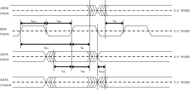 Figure 2. PCM514x Serial Audio Timing - Slave
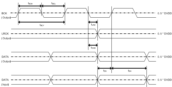 Figure 3. PCM514x Serial Audio Timing - I2S Master
 Figure 4. XSMT Timing for Soft Mute and Soft Un-Mute
7.10 Typical Characteristics
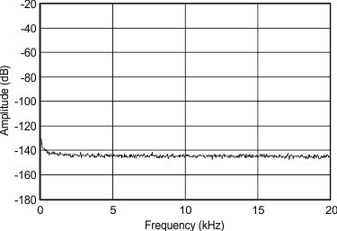
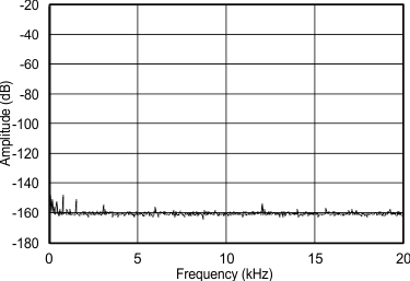
Consumer grade (non-Q1) devices are specified for TA = 25°C, AVDD = CPVDD = DVDD = 3.3 V, fS = 48 kHz, system clock = 512 fS and 24-bit data (unless otherwise noted).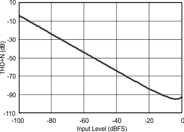
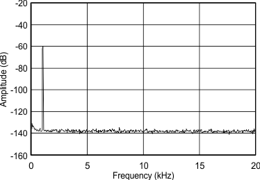
(–60 dBFS) from DC to 20 kHz
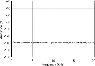

(–60 dBFS) from DC to 300 kHz

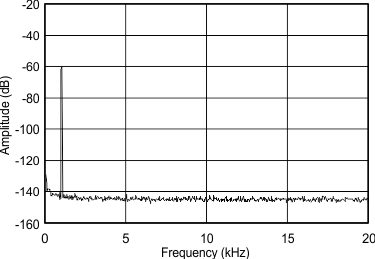
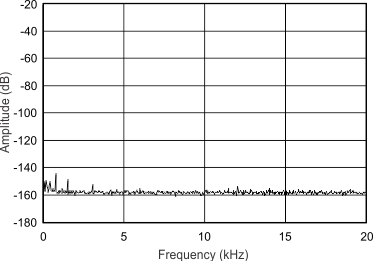
(–60 dBFS) from DC to 20 kHz
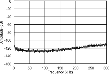
(–60 dBFS) from DC to 300 kHz