-
TPS7A85 High-Current (4 A), High-Accuracy (1%), Low-Noise (4.4 µVRMS), LDO Voltage Regulator
- 1 Features
- 2 Applications
- 3 Description
- 4 Revision History
- 5 Pin Configurations and Functions
- 6 Specifications
- 7 Detailed Description
-
8 Application and Implementation
- 8.1
Application Information
- 8.1.1 Recommended Capacitor Types
- 8.1.2 Input and Output Capacitor Requirements (CIN and COUT)
- 8.1.3 Noise-Reduction and Soft-Start Capacitor (CNR/SS)
- 8.1.4 Feed-Forward Capacitor (CFF)
- 8.1.5 Soft-Start and In-Rush Current
- 8.1.6 Optimizing Noise and PSRR
- 8.1.7 ANY-OUT Programmable Output Voltage
- 8.1.8 ANY-OUT Operation
- 8.1.9 Increasing ANY-OUT Resolution for LILO Conditions
- 8.1.10 Current Sharing
- 8.1.11 Adjustable Operation
- 8.1.12 Sequencing Requirements
- 8.1.13 Power-Good (PG) Operation
- 8.1.14 Undervoltage Lockout (UVLO) Operation
- 8.1.15 Dropout Voltage (VDO)
- 8.1.16 Behavior when Transitioning from Dropout into Regulation
- 8.1.17 Load Transient Response
- 8.1.18 Negatively-Biased Output
- 8.1.19 Reverse Current Protection
- 8.1.20 Power Dissipation (PD)
- 8.2 Typical Applications
- 8.1
Application Information
- 9 Power-Supply Recommendations
- 10Layout
- 11Device and Documentation Support
- 12Mechanical, Packaging, and Orderable Information
- IMPORTANT NOTICE
TPS7A85 High-Current (4 A), High-Accuracy (1%), Low-Noise (4.4 µVRMS), LDO Voltage Regulator
1 Features
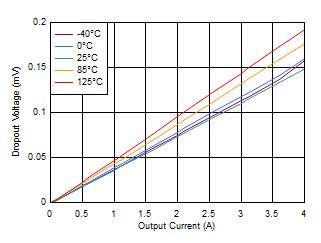
- Low Dropout: 150 mV (typ) at 4 A
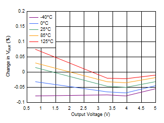
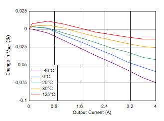
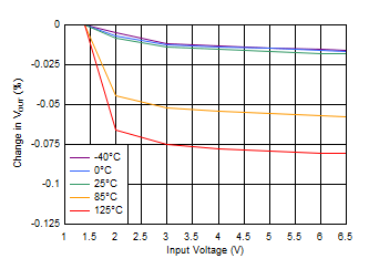
- 1% (max) Accuracy Over Line, Load, and Temperature
- Output Voltage Noise:
- 4.4 µVRMS at 0.8-V Output
- 8.4 µVRMS at 5.0-V Output
- Input Voltage Range:
- Without BIAS: 1.4 V to 6.5 V
- With BIAS: 1.1 V to 6.5 V
- ANY-OUT™ Operation:
- Output Voltage Range: 0.8 V to 3.95 V
- Adjustable Operation:
- Output Voltage Range: 0.8 V to 5.0 V
- Power-Supply Ripple Rejection:
- 40 dB at 500 kHz
- Excellent Load Transient Response
- Adjustable Soft-Start In-Rush Control
- Open-Drain Power-Good (PG) Output
- Stable with a 47-µF or Larger Ceramic Output Capacitor
- Operating Temperature Range:
–40ºC to +125°C - 3.5-mm × 3.5-mm, 20-Pin VQFN
2 Applications
- Digital Loads: SerDes, FPGAs, and DSPs
- Instrumentation, Medical, and Audio
- High-Speed Analog Circuits:
- VCO, ADC, DAC, and LVDS
- Imaging: CMOS Sensors and Video ASICs
- Test and Measurement
3 Description
The TPS7A85 is a low-noise (4.4 µVRMS), low-dropout linear regulator (LDO) capable of sourcing 4 A with only 240 mV of maximum dropout. The device output voltage is pin-programmable from 0.8 V to 3.95 V and adjustable from 0.8 V to 5.0 V using an external resistor divider.
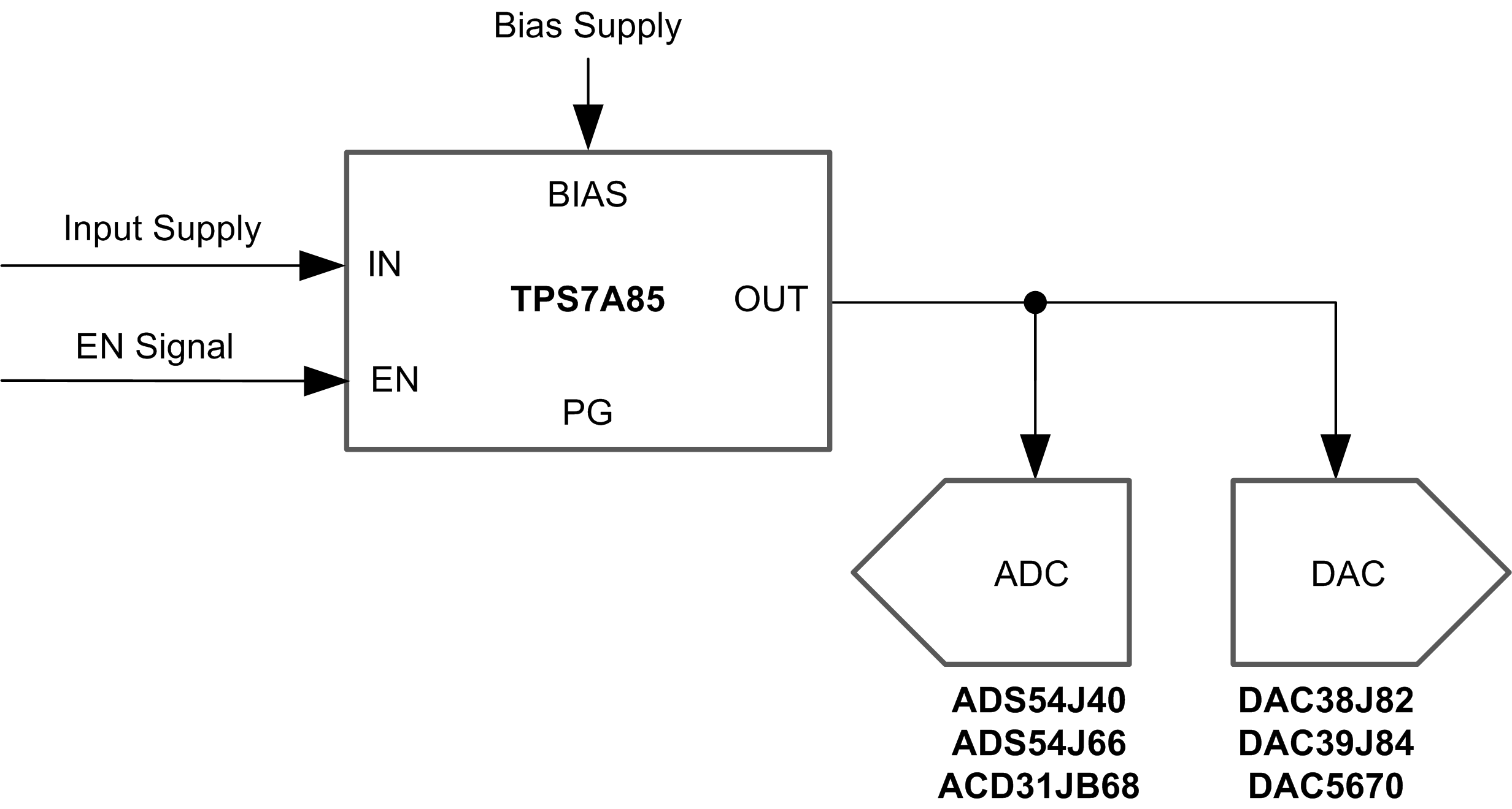
The combination of low-noise (4.4 µVRMS), high-PSRR, and high output current capability makes the TPS7A85 ideal to power noise-sensitive components such as those found in high-speed communications, video, medical, or test and measurement applications. The high performance of the TPS7A85 limits power-supply-generated phase noise and clock jitter, making this device ideal for powering high-performance serializer and deserializer (SerDes), analog-to-digital converters (ADCs), digital-to-analog converters (DACs), and RF components. Specifically, RF amplifiers benefit from the high-performance and 5.0-V output capability of the device.
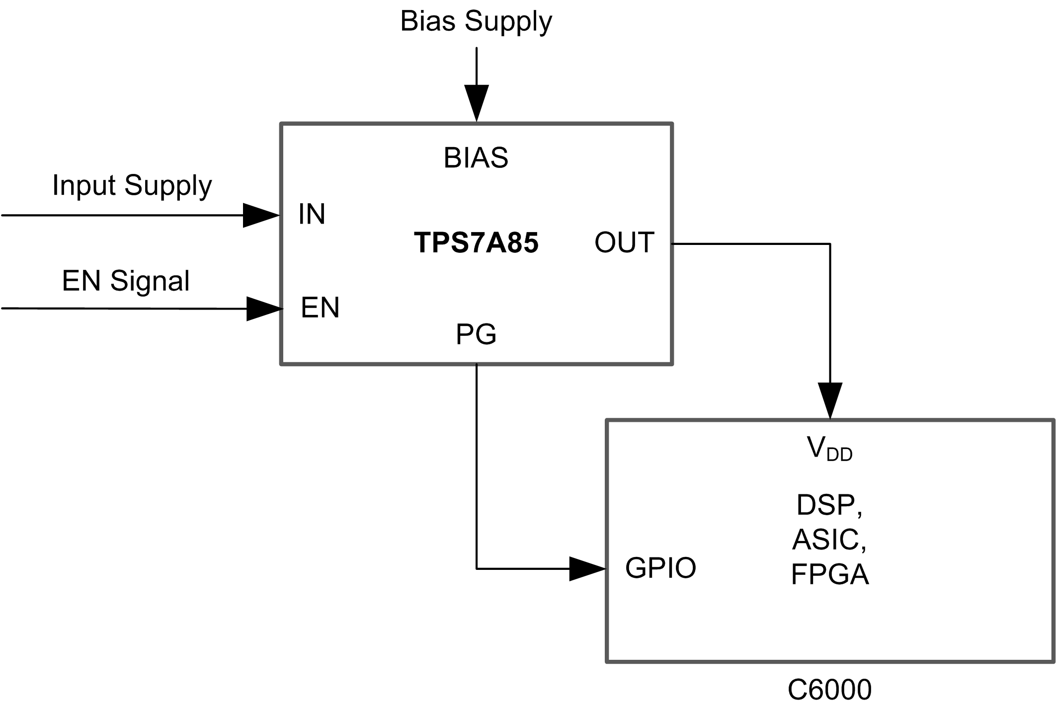
For digital loads [such as application-specific integrated circuits (ASICs), field-programmable gate arrays (FPGAs), and digital signal processors (DSPs)] requiring low-input voltage, low-output (LILO) voltage operation, the exceptional accuracy (0.75% over load and temperature), remote sensing, excellent transient performance, and soft-start capabilities of the TPS7A85 ensure optimal system performance.
The versatility of the TPS7A85 makes the device a component of choice for many demanding applications.
Device Information(1)
| PART NUMBER | PACKAGE | BODY SIZE (nom) |
|---|---|---|
| TPS7A85 | VQFN (20) | 3.50 mm × 3.50 mm |
- For all available packages, see the orderable addendum at the end of the datasheet.
Powering RF Components
Powering Digital Loads
5 Pin Configurations and Functions
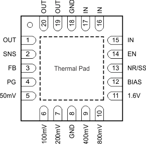
Pin Functions
| PIN | DESCRIPTION | ||
|---|---|---|---|
| NAME | NO. | I/O | |
| 50mV | 5 | I | ANY-OUT voltage setting pins. Connect these pins to ground, SNS, or leave floating. Connecting these pins to ground increases the output voltage, whereas connecting these pins to SNS increases the resolution of the ANY-OUT network but decreases the range of the network; multiple pins can be simultaneously connected to GND or SNS to select the desired output voltage. Leave these pins floating (open) when not in use. See the ANY-OUT Programmable Output Voltage section for additional details. |
| 100mV | 6 | ||
| 200mV | 7 | ||
| 400mV | 9 | ||
| 800mV | 10 | ||
| 1.6V | 11 | ||
| BIAS | 12 | I | BIAS supply voltage. This pin enables the use of low-input voltage, low-output (LILO) voltage conditions (that is, VIN = 1.2 V, VOUT = 1 V) to reduce power dissipation across the die. The use of a BIAS voltage improves dc and ac performance for VIN ≤ 2.2 V. A 10-µF capacitor or larger must be connected between this pin and ground. If not used, this pin must be left floating or tied to ground. |
| EN | 14 | I | Enable pin. Driving this pin to logic high enables the device; driving this pin to logic low disables the device. If enable functionality is not required, this pin must be connected to IN. If enable functionality is required, VEN must always be high after VIN is established when a BIAS supply is used. See the Sequencing Requirements section for more details. |
| FB | 3 | I | Feedback pin connected to the error amplifier. Although not required, a 10-nF feed-forward capacitor from FB to OUT (as close to the device as possible) is recommended to maximize ac performance. The use of a feed-forward capacitor can disrupt PG (power good) functionality. See the ANY-OUT Programmable Output Voltage and Adjustable Operation sections for more details. |
| GND | 8, 18 | — | Ground pin. These pins must be connected to ground, the thermal pad, and each other with a low-impedance connection. |
| IN | 15-17 | I | Input supply voltage pins. A 47-μF or larger ceramic capacitor (25 μF or greater of effective capacitance) from IN to ground is recommended to reduce the impedance of the input supply. Place the input capacitor as close to the input as possible. See the Input and Output Capacitor Requirements section for more details. |
| NR/SS | 13 | — | Noise-reduction and soft-start pin. Connecting an external capacitor between this pin and ground reduces reference voltage noise and also enables the soft-start function. Although not required, a 10-nF or larger capacitor is recommended to be connected from NR/SS to GND (as close to the pin as possible) to maximize ac performance. See the Noise-Reduction and Soft-Start Capacitor section for more details. |
| OUT | 1, 19, 20 | O | Regulated output pins. A 47-μF or larger ceramic capacitor (25 μF or greater of effective capacitance) from OUT to ground is required for stability and must be placed as close to the output as possible. Minimize the impedance from the OUT pin to the load. See the Input and Output Capacitor Requirements section for more details. |
| PG | 4 | O | Active-high, power-good pin. An open-drain output indicates when the output voltage reaches 89.3% of the target. The use of a feed-forward capacitor can disrupt PG (power good) functionality. See the Power-Good (PG) Function section for more details. |
| SNS | 2 | I | Output voltage sense input pin. This pin connects the internal R1 resistor to the output. Connect this pin to the load side of the output trace only if the ANY-OUT feature is used. If the ANY-OUT feature is not used, leave this pin floating. See the ANY-OUT Programmable Output Voltage and Adjustable Operation sections for more details. |
| Thermal pad | — | Connect the thermal pad to a large-area ground plane. The thermal pad is internally connected to GND. | |
6 Specifications
6.1 Absolute Maximum Ratings
over junction temperature range (unless otherwise noted)(1)| MIN | MAX | UNIT | ||
|---|---|---|---|---|
| Voltage | IN, BIAS, PG, EN | –0.3 | 7.0 | V |
| IN, BIAS, PG, EN (5% duty cycle, pulse duration = 200 µs) | –0.3 | 7.5 | ||
| SNS, OUT | –0.3 | VIN + 0.3(2) | ||
| NR/SS, FB | –0.3 | 3.6 | ||
| 50mV, 100mV, 200mV, 400mV, 800mV, 1.6V | –0.3 | VOUT + 0.3 | ||
| Current | OUT | Internally limited | A | |
| PG (sink current into device) | 5 | mA | ||
| Operating junction temperature, TJ | –55 | 150 | °C | |
| Storage temperature, Tstg | –55 | 150 | °C | |
6.2 ESD Ratings
| VALUE | UNIT | |||
|---|---|---|---|---|
| V(ESD) | Electrostatic discharge | Human-body model (HBM), per ANSI/ESDA/JEDEC JS-001(1) | ±2000 | V |
| Charged-device model (CDM), per JEDEC specification JESD22-C101(2) | ±500 | |||
6.3 Recommended Operating Conditions
over junction temperature range (unless otherwise noted)| MIN | NOM | MAX | UNIT | ||
|---|---|---|---|---|---|
| VIN | Input supply voltage range | 1.1 | 6.5 | V | |
| VBIAS | Bias supply voltage range(1) | 3.0 | 6.5 | V | |
| VOUT | Output voltage range(2) | 0.8 | 5 | V | |
| VEN | Enable voltage range | 0 | VIN | V | |
| IOUT | Output current | 0 | 4 | A | |
| CIN | Input capacitor | 10 | 47 | µF | |
| COUT | Output capacitor | 47 | 47 || 10 || 10(3) | µF | |
| RPG | Power-good pullup resistance | 10 | 100 | kΩ | |
| CNR/SS | NR/SS capacitor | 10 | nF | ||
| CFF | Feed-forward capacitor | 10 | nF | ||
| R1 | Top resistor value in feedback network for adjustable operation | 12.1(4) | kΩ | ||
| R2 | Bottom resistor value in feedback network for adjustable operation | 160(5) | kΩ | ||
| TJ | Operating junction temperature | –40 | 125 | °C | |
6.4 Thermal Information
| THERMAL METRIC(1) | TPS7A85 | UNIT | |
|---|---|---|---|
| RGR (VQFN) | |||
| 20 PINS | |||
| RθJA | Junction-to-ambient thermal resistance | 35.4 | °C/W |
| RθJC(top) | Junction-to-case (top) thermal resistance | 47.6 | °C/W |
| RθJB | Junction-to-board thermal resistance | 12.3 | °C/W |
| ψJT | Junction-to-top characterization parameter | 0.5 | °C/W |
| ψJB | Junction-to-board characterization parameter | 12.4 | °C/W |
| RθJC(bot) | Junction-to-case (bottom) thermal resistance | 1.0 | °C/W |
6.5 Electrical Characteristics
Over operating junction temperature range (TJ = –40°C to +125°C), VIN = 1.4 V or VIN = VOUT(nom) + 0.5 V (whichever is greater), VBIAS = open, VOUT(nom) = 0.8 V(2), OUT connected to 50 Ω to GND(3), VEN = 1.1 V, CIN = 10 μF, COUT = 47 μF, CNR/SS without CFF, and PG pin pulled up to VIN with 100 kΩ, unless otherwise noted. Typical values are at TJ = 25°C.| PARAMETER | TEST CONDITIONS | MIN | TYP | MAX | UNIT | |||
|---|---|---|---|---|---|---|---|---|
| VIN | Input supply voltage range(1) | 1.1 | 6.5 | V | ||||
| VBIAS | Bias supply voltage range(1) | VIN = 1.1 V | 3.0 | 6.5 | V | |||
| VFB | Feedback voltage | 0.8 | V | |||||
| VNR/SS | NR/SS pin voltage | 0.8 | V | |||||
| VUVLO1(IN) | Input supply UVLO with BIAS | VIN rising with VBIAS = 3.0 V | 1.02 | 1.085 | V | |||
| VHYS1(IN) | VUVLO1(IN) hysteresis | VBIAS = 3.0 V | 320 | mV | ||||
| VUVLO2(IN) | Input supply UVLO without BIAS | VIN rising | 1.31 | 1.39 | V | |||
| VHYS2(IN) | VUVLO2(IN) hysteresis | 253 | mV | |||||
| VUVLO(BIAS) | Bias supply UVLO | VBIAS rising, VIN = 1.1 V | 2.83 | 2.9 | V | |||
| VHYS(BIAS) | VUVLO(BIAS) hysteresis | VIN = 1.1 V | 290 | mV | ||||
| VOUT | Output voltage | Range | Using the ANY-OUT pins | 0.8 – 1.0% | 3.95 + 1.0% | V | ||
| Using external resistors(4) | 0.8 – 1.0% | 5.0 + 1.0% | ||||||
| Accuracy(4)(5) | 0.8 V ≤ VOUT ≤ 5 V, 5 mA ≤ IOUT ≤ 4 A, over VIN | –1.0% | 1.0% | |||||
| Accuracy with BIAS | VIN = 1.1 V, 5 mA ≤ IOUT ≤ 4 A, 3.0 V ≤ VBIAS ≤ 6.5 V |
–0.75% | 0.75% | |||||
| ΔVOUT/ ΔVIN |
Line regulation | IOUT = 5 mA, 1.4 V ≤ VIN ≤ 6.5 V | 0.0035 | mV/V | ||||
| ΔVOUT/ ΔIOUT |
Load regulation | 5 mA ≤ IOUT ≤ 4 A, 3.0 V ≤ VBIAS ≤ 6.5 V, VIN = 1.1 V |
0.07 | mV/A | ||||
| 5 mA ≤ IOUT ≤ 4 A | 0.08 | |||||||
| 5 mA ≤ IOUT ≤ 4 A, VOUT = 5.0 V | 0.4 | |||||||
| VDO | Dropout voltage | VIN = 1.4 V, IOUT = 4 A, VFB = 0.8 V – 3% | 215 | 320 | mV | |||
| VIN = 5.5 V, IOUT = 4 A, VFB = 0.8 V – 3% | 325 | 500 | ||||||
| VIN = 1.1 V, VBIAS = 5.0 V, IOUT = 4 A, VFB = 0.8 V – 3% |
150 | 240 | ||||||
| ILIM | Output current limit | VOUT forced at 0.9 × VOUT(nom), VIN = VOUT(nom) + 0.4 V |
4.7 | 5.2 | 5.7 | A | ||
| ISC | Short-circuit current limit | RLOAD = 20 mΩ | 1.0 | A | ||||
| IGND | GND pin current | VIN = 6.5 V, IOUT = 5 mA | 2.8 | 4.0 | mA | |||
| VIN = 1.4 V, IOUT = 4 A | 4.8 | 6.0 | ||||||
| Shutdown, PG = open, VIN = 6.5 V, VEN = 0.5 V | 25 | µA | ||||||
| IEN | EN pin current | VIN = 6.5 V, VEN = 0 V and 6.5 V | –0.1 | 0.1 | µA | |||
| IBIAS | BIAS pin current | VIN = 1.1 V, VBIAS = 6.5 V, VOUT(nom) = 0.8 V, IOUT = 4 A |
2.3 | 3.5 | mA | |||
| VIL(EN) | EN pin high-level input voltage (enable device) |
0 | 0.5 | V | ||||
| VIH(EN) | EN pin low-level input voltage (disable device) |
1.1 | 6.5 | V | ||||
| VIT(PG) | PG pin threshold | For falling VOUT | 82% × VOUT | 88.3% × VOUT | 93% × VOUT | V | ||
| VHYS(PG) | PG pin hysteresis | For rising VOUT | 1% × VOUT | V | ||||
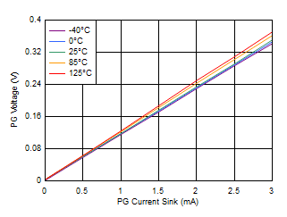
| VOL(PG) | PG pin low-level output voltage | VOUT < VIT(PG), IPG = –1 mA (current sunk into pin) |
0.4 | V | ||||
| Ilkg(PG) | PG pin leakage current | VOUT > VIT(PG), VPG = 6.5 V | 1 | µA | ||||
| INR/SS | NR/SS pin charging current | VNR/SS = GND, VIN = 6.5 V | 4.0 | 6.2 | 9.0 | µA | ||
| IFB | FB pin leakage current | VIN = 6.5 V | –100 | 100 | nA | |||
| PSRR | Power-supply ripple rejection | VIN – VOUT = 0.5 V, IOUT = 4 A, CNR/SS = 100 nF, CFF = 10 nF, COUT = 47 μF || 10 μF || 10 μF |
f = 10 kHz, VOUT = 0.8 V, VBIAS = 5.0 V |
42 | dB | |||
| f = 500 kHz, VOUT = 0.8 V, VBIAS = 5.0 V | 39 | |||||||
| f = 10 kHz, VOUT = 3.3 V |
40 | |||||||
| f = 500 kHz, VOUT = 3.3 V | 25 | |||||||
| Vn | Output noise voltage | BW = 10 Hz to 100 kHz, VIN = 1.2 V, VOUT = 0.8 V, VBIAS = 5.0 V, IOUT = 4 A, CNR/SS = 100 nF, CFF = 10 nF, COUT = 47 μF || 10 μF || 10 μF |
4.4 | μVRMS | ||||
| BW = 10 Hz to 100 kHz, VOUT = 5.0 V, IOUT = 4 A, CNR/SS = 100 nF, CFF = 10 nF, COUT = 47 μF || 10 μF || 10 μF |
8.4 | |||||||
| Tsd | Thermal shutdown temperature | Shutdown, temperature increasing | 160 | °C | ||||
| Reset, temperature decreasing | 140 | |||||||
| TJ | Operating junction temperature | –40 | 125 | °C | ||||
6.6 Typical Characteristics
at TA = 25°C, VIN = 1.4 V or VIN = VOUT(NOM) + 0.5 V (whichever is greater), VBIAS = open, VOUT(NOM) = 0.8 V, VEN = 1.1 V, COUT = 47 μF, CNR/SS = 0 nF, CFF = 0 nF, and PG pin pulled up to VIN with 100 kΩ (unless otherwise noted)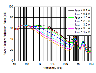
| VIN = 1.2 V, VBIAS = 5 V, COUT = 47 μF || 10 μF || 10 μF, CNR/SS = 10 nF, CFF = 10 nF |
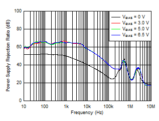
| VIN = 1.4 V, IOUT = 1 A, COUT = 47 μF || 10 μF || 10 μF, CNR/SS = 10 nF, CFF = 10 nF |

| VIN = VOUT + 0.4 V, VBIAS = 5.0 V, IOUT = 4 A, COUT = 47 μF || 10 μF || 10 μF, CNR/SS = 10 nF, CFF = 10 nF |

| VIN = 5.6 V, COUT = 47 μF || 10 μF || 10 μF, CNR/SS = 10 nF, CFF = 10 nF |
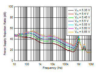
| IOUT = 4 A, COUT = 47 μF || 10 μF || 10 μF, CNR/SS = 10 nF, CFF = 10 nF |
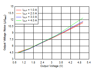
| VIN = VOUT + 0.4 V and VBIAS = 5 V for VOUT ≤ 2.2 V,
COUT = 47 μF || 10 μF || 10 μF, CNR/SS = 10 nF, CFF = 10 nF |
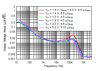
| IOUT = 1 A, COUT = 47 μF || 10 μF || 10 μF, CNR/SS = 10 nF, CFF = 10 nF |
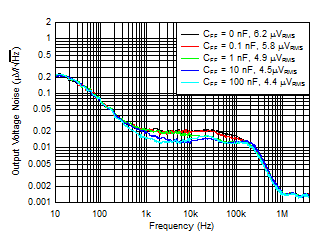
| VIN = VOUT + 0.4 V, VBIAS = 5 V, IOUT = 4 A, COUT = 47 μF || 10 μF || 10 μF, CNR/SS = 10 nF |

| VIN = 1.2 V, VOUT = 0.9 V, VBIAS = 5.0 V, IOUT = 4 A, COUT = 47 μF || 10 μF || 10 μF, CFF = 10 nF |
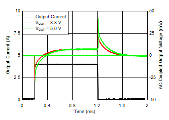
| IOUT, DC = 100 mA, COUT = 47 μF || 10 μF || 10 μF, CNR/SS = CFF = 10 nF, slew rate = 1 A/μs |
VOUT without Bias
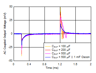
| VIN = 1.2 V, VBIAS = 5.0 V, IOUT = 100 mA to 4 A, CNR/SS = CFF = 10 nF, slew rate = 1 A/μs |
(VOUT = 0.9 V)
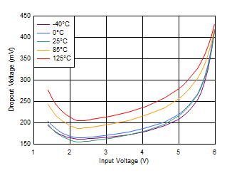
| IOUT = 4 A, VBIAS = 0 V |
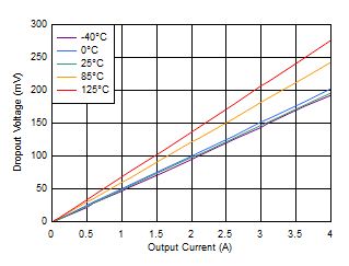
| VIN = 1.4 V, VBIAS = 0 V |

| VIN = 5.5 V |
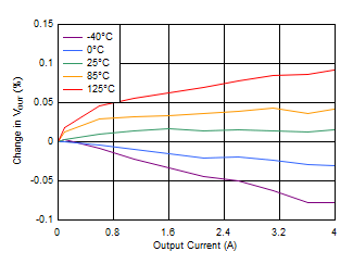
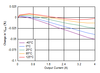
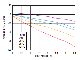
| VIN = 1.1 V, IOUT = 5 mA |
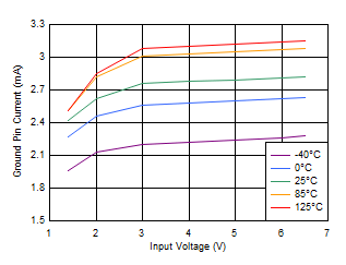
| IOUT = 5 mA |
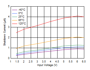
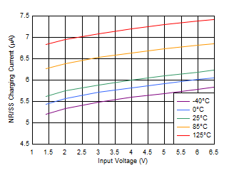

| VIN = 1.1 V |
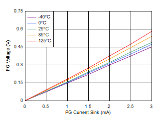
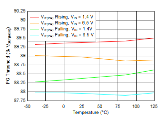

| IOUT = 4 A, VBIAS = 5 V, COUT = 47 μF || 10 μF || 10 μF, CNR/SS = 10 nF, CFF = 10 nF |
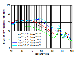
| IOUT = 1 A, COUT = 47 μF || 10 μF || 10 μF, CNR/SS = 10 nF, CFF = 10 nF |
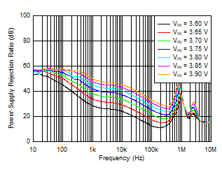
| IOUT = 4 A, COUT = 47 μF || 10 μF || 10 μF, CNR/SS = 10 nF, CFF = 10 nF |
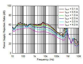
| VIN = VOUT + 0.4 V, VOUT = 1 V, IOUT = 4 A,
COUT = 47 μF || 10 μF || 10 μF, CNR/SS = 10 nF, CFF = 10 nF |
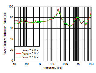
| VIN = VOUT + 0.4 V, VOUT = 1 V, IOUT = 4 A,
COUT = 47 μF || 10 μF || 10 μF, CNR/SS = 10 nF, CFF = 10 nF |
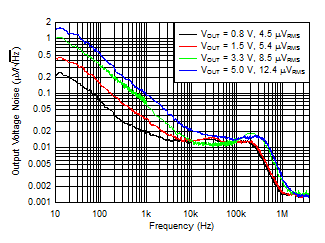
| VIN = VOUT + 0.4 V and VBIAS = 5 V for VOUT ≤ 2.2 V, IOUT = 4 A, COUT = 47 μF || 10 μF || 10 μF, CNR/SS = 10 nF, CFF = 10 nF |
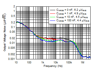
| VIN = VOUT + 0.4 V, VBIAS = 5 V, IOUT = 4 A, COUT = 47 μF || 10 μF || 10 μF, CFF = 10 nF |
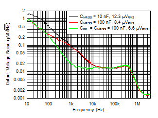
| VIN = 5.6 V, IOUT = 4 A, COUT = 47 μF || 10 μF || 10 μF, CFF = 10 nF |
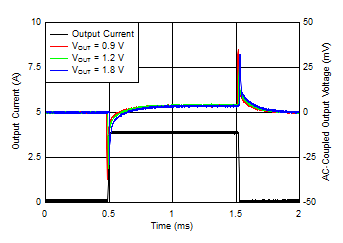
| VIN = VOUT + 0.3 V, VBIAS = 5 V, IOUT, DC = 100 mA, slew rate = 1 A/μs, CNR/SS = CFF = 10 nF, COUT = 47 μF || 10 μF || 10 μF |
VOUT with Bias
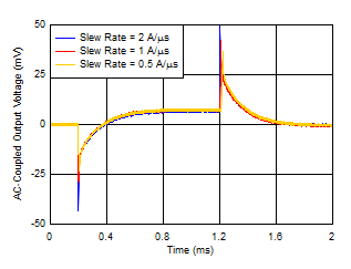
| VOUT = 5 V, IOUT, DC = 100 mA, IOUT = 100 mA to 4 A, COUT = 47 μF || 10 μF || 10 μF, CNR/SS = CFF = 10 nF |
Slew Rate
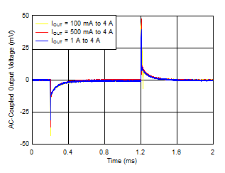
| VIN = 1.2 V, VBIAS = 5.0 V, COUT = 47 μF || 10 μF || 10 μF, CNR/SS = CFF = 10 nF, slew rate = 1 A/μs |
(VOUT = 0.9 V)
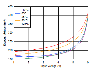
| IOUT = 4 A, VBIAS = 6.5 V |
| VIN = 1.1 V, VBIAS = 3 V |
| IOUT = 100 mA to 4 A |
| IOUT = 5 mA |
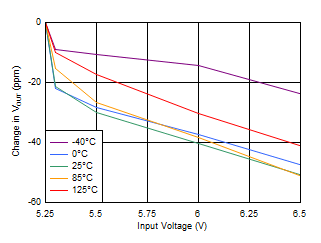
| IOUT = 5 mA |
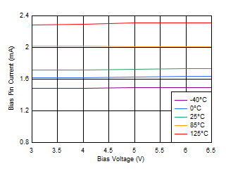
| VIN = 1.1 V, IOUT = 5 mA |
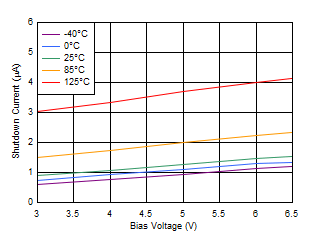
| VIN = 1.1 V |

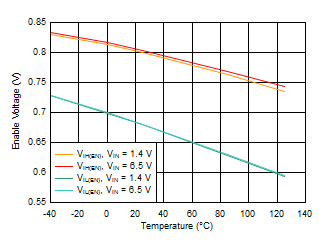
| VIN = 6.5 V |