SBOA512 April 2021 INA901-SP
Design Goals
| Input | Overcurrent Conditions | Output | Supply | Response Time | Total Ionizing Dose | Single Event Immunity | |
|---|---|---|---|---|---|---|---|
| Iload Min | Iload Max | IOC_TH | Vout_OC | VS | tdelay | TID | SEL |
| 5A | 10A | 11A | 2.2V | 5V | < 5µs | 50 krad (Si) | 75 MeV×cm2/mg |
Design Description
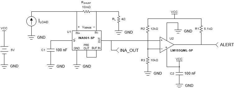
This is a unidirectional current-sensing solution, generally referred to as overcurrent protection (OCP) that can provide an overcurrent alert signal to power off a system exceeding a threshold current. In this particular setup, the normal operating load is from 5A to 10A, with the overcurrent threshold defined at 11A (IOC_TH). The current shunt monitor and comparator are powered from a single 5-V supply rail. OCP can be applied to both high-side and low-side topologies. The solution presented in this circuit is a high-side implementation, with RL placed as a representation of a purely resistive system load at 4Ω. This circuit is useful in a variety of power applications for telemetry, health monitoring and system diagnostics. In addition to this functionality, this circuit implements the INA901-SP, which is a Radiation-Hardness-Assured (RHA), 50-krad(Si) capable device at Low Dose Rate, that is also Single Event Latch-up (SEL) Immune to 75 MeV-cm2/mg at 125°C. The comparator function is fulfilled by a LM193QML-SP, but the LM139AQML-SP can be used here as well, if additional comparator device count is needed.
Design Notes
- For accurate comparator applications without hysteresis, it is important to maintain a stable power supply with minimized noise and glitches. To achieve this, use decoupling capacitors C1 and C2 to ensure device supplies are stable. Place the decoupling capacitors as close as possible to the supply pins of their respective devices. This should also be implemented on the negative supply of the comparator, if used.
- If a larger dynamic current measurement range is required with a higher trip point, a voltage divider from the INA901-SP OUT pin to ground can be incorporated with the divider output going to the LM193QML-SP input. Ensure that the designed range of the INA901-SP remains within the input common-mode specification of the LM193QML-SP.
- If additional short circuit to ground protection is needed in the circuit, fuses in series with the input pins can provide this functionality, but resistors should not be used for this purpose. Addition of resistors to the input pins of the INA901-SP will fundamentally change the gain of the amplifier. However, the tolerance of the internal resistors will fluctuate up to 30% (these resistors are matched to one another, rather than an absolute value), and thus this change in gain will vary from device to device, and cannot be considered reliable design.
Design Steps
- Full Scale Range: Determine the load range of conditions needing to be monitored. Choice of RSHUNT should be made with respect to the maximum range of current allowable to the input sense voltage, including the overcurrent value. Additional considerations are offset voltage on the lower end of measurement, and maintaining a valid common mode voltage on the input pins of the LM193QML-SP. While designing with INA901-SP, for best performance, ensure that the IMIN condition with the chosen shunt produces a sense voltage > 20mV to comply with the Accuracy Variations as a Result of VSENSE and Common-Mode Voltage section of the INA901-SP Radiation Hardened, –15-V to 65-V Common Mode, Unidirectional Current-Shunt Monitor Data Sheet.
- Gain Options: For the INA901-SP, only a 20V/V option is available, so this condition is fixed for this design.
- Choosing a shunt resistor: Given the design conditions, choose an appropriate shunt using the following equation. Note that there is a 200-mV reduction on the supply voltage to ensure that the device meets swing-to-rail limitations of the device. Numerical values come from the previously-defined use case:Equation 1.
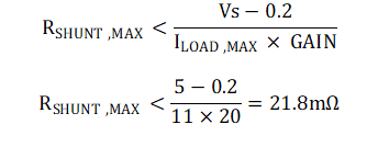
A shunt resistor value of 10mΩ is chosen for the design. Be aware that while a larger shunt provides more utilization of the full scale range, thermal constraints on the shunt will increase proportionally with the resistance. Selection of a higher value will also increase the voltage of the overcurrent trip point, which may cause challenges in satisfying the common-mode requirement of the LM193QML-SP.
- Setting the overcurrent point: From the INA901-SP, with the value of RSHUNT now determined, it is found that the output of the INA901-SP at the overcurrent point is:Equation 1.
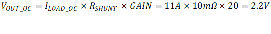
The overcurrent condition is set by a voltage divider between R2 and R3 set for the previously-mentioned point. Choose a value for R3 and calculate the needed resistor R2. Here, R3 is chosen at 10kΩ:
Equation 1.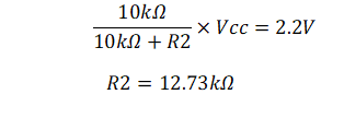
Note that the LM193QML-SP requires that at least one input be from 0V to 3V when operating at a supply of 5V to satisfy the input common-mode requirement. This node held at a constant 2.2V satisfies this requirement for all values of comparison.
Often, calculated resistor values will not directly align with available resistor choices. Here, 12.73kΩ is not a standard value, so the closest standard value of 12kΩ is selected. The actual overcurrent point based on the resistor value can be found by combining the previous equations.
Equation 1.
- Offset error check: Check that the minimum meaningful current measurement is significantly higher than the current shunt monitor input offset voltage. The recommended maximum error from offset, eVOS is 10%. The value of eVOS can be lowered for tighter error targets: Equation 1.
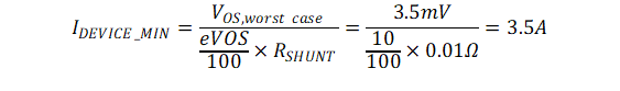
This value means that at a measured current of 3.5A for the chosen shunt, offset voltage will contribute a 10% error to the measurement.
Design Simulations
Transient Simulation Results
High-Side OCP Simulation Results
The first simulation examines the ramp response of the circuit, as the current transitions above the overcurrent trigger point.
 INA901-SP Overcurrent Ramp Response
 INA901-SP Overcurrent Ramp Response, Zoom In
Next, examining the delay response of the circuit, with a step response delivered at 4.0ms, it is shown that the circuit responds to the event approximately 2.5µs later, so the delay response is satisfied:
 INA901-SP Overcurrent Protection Step Response
Design References
See the TI Precision Labs, Current Sense Amplifiers video series.
| INA901-SP | |
|---|---|
| VS | 2.7V to 16V |
| VCM | –15V to 65V |
| VOUT | GND+3mV to VS-50mV, typical |
| VOS | ±500μV, typical |
| Iq | 350μA, typical |
| IB | ±8μA, typical |
TID Characterization (ELDRS-Free) | 50krad (Si) |
SEL Immune to LET | 75 MeV-cm2/mg |
| https://www.ti.com/product/INA901-SP | |
For less harsh radiation environments, TI also offers the INA240-SEP, which offers Single Event Latch-up (SEL) Immunity to 43 MeV-cm2/mg at 125°C. It is ELDRS Free to 30 krad(Si), and Total Ionizing Dose (TID) RLAT for Every Wafer Lot is up to 20 krad(Si):
| INA240-SEP | |
|---|---|
| VS | 2.7V to 5.5V |
| VCM | –4V to 80V |
| VOUT | GND+1mV to VS-50mV, typical |
| VOS | ±5μV, typical |
| Iq | 1.8mA, typical |
| IB | ±90μA, typical |
TID Characterization (ELDRS-Free) | 30 krad (Si) |
SEL Immune to LET | 43 MeV-cm2/mg |
| https://www.ti.com/product/INA240-SEP | |
TLV1704-SEP | LM139AQML-SP | |
|---|---|---|
| VS | 2.2V to 36V | 2V to 36V |
| VCM | Rail-to-Rail | 0V to 34V |
| VOUT | Open-Collector, Rail-to-Rail | Open-Collector |
| VOS | 500μV | 2mV |
| Iq | 55μA/channel | 200μA/channel |
tPD(HL) | 460ns | 2.50μs |
TID Characterization (ELDRS-Free) | 30 krad (Si) | 100 krad (Si) |
SEL Immune to LET | 43 MeV-cm2/mg | SEL Immune (Bipolar process) |
| https://www.ti.com/product/LM139AQML-SP |