• Menu
  • Product
  • Email
  • PDF
  • Order now
  • LMG341xR070 600-V 70-mΩ GaN with Integrated Driver and Protection

    • SNOSD10F April   2016  – May 2020

      PRODUCTION DATA.  

  • CONTENTS
  • SEARCH
  • LMG341xR070 600-V 70-mΩ GaN with Integrated Driver and Protection
  1. 1 Features
  2. 2 Applications
  3. 3 Description
    1.     Device Images
      1.      Simplified Block Diagram
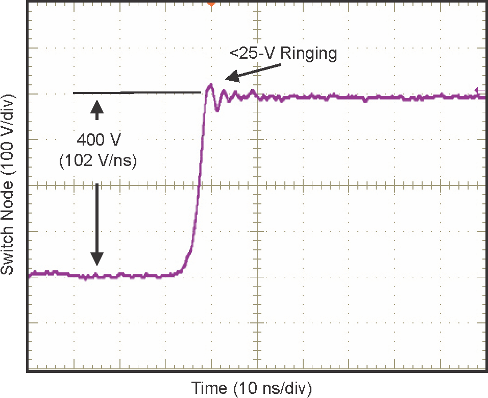
      2.      Switching Performance at >100 V/ns
  4. 4 Revision History
  5. 5 Pin Configuration and Functions
    1.     Pin Functions
  6. 6 Specifications
    1. 6.1 Absolute Maximum Ratings
    2. 6.2 ESD Ratings
    3. 6.3 Recommended Operating Conditions
    4. 6.4 Thermal Information
    5. 6.5 Electrical Characteristics
    6. 6.6 Switching Characteristics
    7. 6.7 Typical Characteristics
  7. 7 Parameter Measurement Information
    1. 7.1 Switching Parameters
      1. 7.1.1 Turn-on Delays
      2. 7.1.2 Turn-off Delays
      3. 7.1.3 Drain Slew Rate
      4. 7.1.4 Turn-on and Turn-off Energy
  8. 8 Detailed Description
    1. 8.1 Overview
    2. 8.2 Functional Block Diagram
    3. 8.3 Feature Description
      1. 8.3.1 Direct-Drive GaN Architecture
      2. 8.3.2 Internal Buck-Boost DC-DC Converter
      3. 8.3.3 Internal Auxiliary LDO
      4. 8.3.4 Fault Detection
        1. 8.3.4.1 Over-current Protection
        2. 8.3.4.2 Over-Temperature Protection and UVLO
      5. 8.3.5 Drive Strength Adjustment
    4. 8.4 Device Functional Modes
      1. 8.4.1 Low-Power Mode
  9. 9 Application and Implementation
    1. 9.1 Application Information
    2. 9.2 Typical Application
      1. 9.2.1 Design Requirements
      2. 9.2.2 Detailed Design Procedure
        1. 9.2.2.1 Slew Rate Selection
          1. 9.2.2.1.1 Startup and Slew Rate with Bootstrap High-Side Supply
        2. 9.2.2.2 Signal Level-Shifting
        3. 9.2.2.3 Buck-Boost Converter Design
      3. 9.2.3 Application Curves
    3. 9.3 Paralleling GaN Devices
    4. 9.4 Do's and Don'ts
  10. 10Power Supply Recommendations
    1. 10.1 Using an Isolated Power Supply
    2. 10.2 Using a Bootstrap Diode
      1. 10.2.1 Diode Selection
      2. 10.2.2 Managing the Bootstrap Voltage
      3. 10.2.3 Reliable Bootstrap Start-up
  11. 11Layout
    1. 11.1 Layout Guidelines
      1. 11.1.1 Power Loop Inductance
      2. 11.1.2 Signal Ground Connection
      3. 11.1.3 Bypass Capacitors
      4. 11.1.4 Switch-Node Capacitance
      5. 11.1.5 Signal Integrity
      6. 11.1.6 High-Voltage Spacing
      7. 11.1.7 Thermal Recommendations
    2. 11.2 Layout Example
  12. 12Device and Documentation Support
    1. 12.1 Device Support
      1. 12.1.1 Third-Party Products Disclaimer
    2. 12.2 Documentation Support
      1. 12.2.1 Related Documentation
    3. 12.3 Receiving Notification of Documentation Updates
    4. 12.4 Community Resources
    5. 12.5 Trademarks
    6. 12.6 Electrostatic Discharge Caution
    7. 12.7 Glossary
  13. 13Mechanical, Packaging, and Orderable Information
  14. IMPORTANT NOTICE
search No matches found.
  • Full reading width
    • Full reading width
    • Comfortable reading width
    • Expanded reading width
  • Card for each section
  • Card with all content


DATA SHEET

LMG341xR070 600-V 70-mΩ GaN with Integrated Driver and Protection

1 Features

  • TI GaN Process Qualified Through Accelerated Reliability In-application Hard-switching Mission Profiles
  • Enables High Density Power Conversion Designs
    • Superior System Performance Over Cascode or Stand-alone GaN FETs
    • Low Inductance 8mm x 8mm QFN Package for Ease of Design, and Layout
    • Adjustable Drive Strength for Switching Performance and EMI Control
    • Digital Fault Status Output Signal
    • Only +12 V Unregulated Supply Needed
  • Integrated Gate Driver
    • Zero Common Source Inductance
    • 20 ns Propagation Delay for MHz Operation
    • Process-tuned Gate Bias Voltage for Reliability
    • 25 to 100V/ns User Adjustable Slew Rate
  • Robust Protection
    • Requires No External Protection Components
    • Over-current Protection with <100ns Response
    • >150V/ns Slew Rate Immunity
    • Transient Overvoltage Immunity
    • Overtemperature Protection
    • UVLO Protection on All Supply Rails
  • Device Options:
    • LMG3410R070: Latched Overcurrent Protection
    • LMG3411R070: Cycle-by-cycle Overcurrent Protection

2 Applications

  • High Density Industrial and Consumer Power Supplies
  • Multi-level Converters
  • Solar Inverters
  • Industrial Motor Drives
  • Uninterruptable Power Supplies
  • High Voltage Battery Chargers

3 Description

The LMG341xR070 GaN power stage with integrated driver and protection enables designers to achieve new levels of power density and efficiency in power electronics systems. The LMG341x’s inherent advantages over silicon MOSFETs include ultra-low input and output capacitance, zero reverse recovery to reduce switching losses by as much as 80%, and low switch node ringing to reduce EMI. These advantages enable dense and efficient topologies like the totem-pole PFC.

The LMG341xR070 provides a smart alternative to traditional cascode GaN and standalone GaN FETs by integrating a unique set of features to simplify design, maximize reliability and optimize the performance of any power supply. Integrated gate drive enables 100V/ns switching with near zero Vds ringing, <100 ns current limiting self-protects against unintended shoot-through events, Overtemperature shutdown prevents thermal runaway, and system interface signals provide self-monitoring capability.

Device Information(1)

PART NUMBER PACKAGE BODY SIZE (NOM)
LMG341xR070 QFN (32) 8.00 mm × 8.00 mm
  1. For all available packages, see the orderable addendum at the end of the data sheet.

Device Images

Simplified Block Diagram
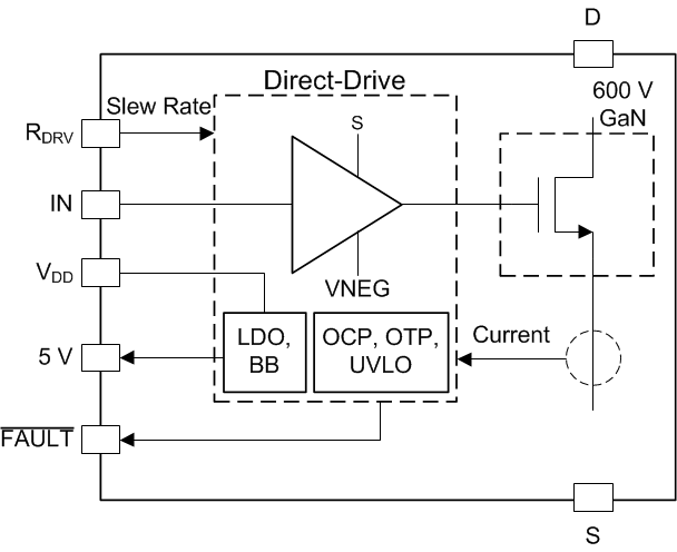
LMG3410R070 LMG3411R070 LMG3410R070-simplified-block-diagram-SNOSD10.gif

Switching Performance at >100 V/ns

LMG3410R070 LMG3411R070 waveform-01-GaN-PowerStage-snosd10.png


Texas Instruments

© Copyright 1995-2025 Texas Instruments Incorporated. All rights reserved.
Submit documentation feedback | IMPORTANT NOTICE | Trademarks | Privacy policy | Cookie policy | Terms of use | Terms of sale