LMX2581 Wideband Frequency Synthesizer with Integrated VCO
1 Features
- Output Frequency from 50 to 3760 MHz
- Input Clock Frequency up to 900 MHz
- Phase Detector Frequency up to 200 MHz
- Supports Fractional and Integer Modes
- –229 dBc/Hz Normalized PLL Phase Noise
- –120.8 dBc/Hz Normalized PLL 1/f Noise
- –137 dBc/Hz VCO Phase Noise @ 1 MHz offset for a 2.5 GHz Carrier
- 100 fs RMS Jitter in Integer Mode
- Programmable Fractional Modulator Order
- Programmable Fractional Denominator
- Programmable Output Power up to +12 dBm
- Programmable 32 Level Charge Pump Current
- Programmable Option to Use an External VCO
- Digital Lock Detect
- 3-Wire Serial Interface and Readback
- Single Supply Voltage from 3.15 V to 3.45 V
- Supports Logic Levels down to 1.6 V
2 Applications
- Wireless Infrastructure (UMTS, LTE, WiMax, Multi-Standard Base Stations)
- Broadband Wireless
- Test and Measurement
- Clock Generation
3 Description
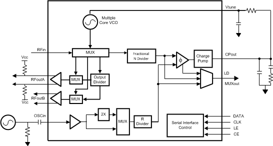
The LMX2581 is a low noise wideband frequency synthesizer that integrates a delta-sigma fractional N PLL, multiple core VCO, programmable output divider, and two differential output buffers. The VCO frequency range is from 1880 to 3760 MHz and can be sent directly to the output buffers or divided down by even values from 2 to 38. Each buffer is capable of output power from -3 to +12 dBm at 2700 MHz. Integrated low noise LDOs are used for superior noise immunity and consistent performance.
This synthesizer is a highly programmable device and it enables the user to optimize its performance. In fractional mode, the denominator and the modulator order are programmable and can be configured with dithering as well. The user also has the ability to directly specify a VCO core or entirely bypass the internal VCO. Finally, many convenient features are included such as power down, Fastlock, auto mute, and lock detection. All registers can be programmed through a simple 3 wire interface and a read back feature is also available.
The LMX2581 operates on a single 3.3 V supply and comes in a 32 pin 5.0 mm × 5.0 mm WQFN package.
Device Information(1)
| PART NUMBER | PACKAGE | BODY SIZE (NOM) |
|---|---|---|
| LMX2581 | WQFN (32) | 5.00 mm × 5.00 mm |
- For all available packages, see the orderable addendum at the end of the datasheet.
4 Simplified Schematic
5 Revision History
Changes from F Revision (March 2014) to G Revision
- Added "over operating free-air temperature range (unless otherwise noted)" in Absolute Maximum Ratings and Recommended Operating Conditions.Go
- Added footnotes to HBM, CDM, and MM in Handling Ratings table.Go
- Moved explanations of Typical Characteristics plots from plot footnotes to Feature Description section.Go
- Moved Impact of Temperature on VCO Phase Noise into Feature Description section.Go
- Added some description of modulator noise floor and Table 4. Go
- Changed -89 to -83 in Table 11Go
- Moved "Triggering Registers" to "Register Maps" section.Go
- Changed order of subsections in Application and Implementation section.Go
- Changed -- inverted color scheme of Figure 23, Figure 24, and Figure 25 to enhance readabilityGo
- Added links for Device and Documentation Support . Added links to Application Note AN-1879 (SNAA062) throughout the document.Go
Changes from E Revision (Novmeber 2013) to F Revision
- Added data sheet structure and organization. Added, updated, or renamed the following sections: Device Information Table, Application and Implementation; Power Supply Recommendations; Layout; Device and Documentation Support; Mechanical, Packaging, and Ordering InformationGo
- Changed Clarified that typical PLL noise metrics are measured at max charge pump gain. Go
- Added Typical Characteristics curves. Go
- Changed Recommendation for OSC_FREQ bit for input frequencies > 64 MHz Go
- Added Application and Implementation section with schematic.Go
- Added Power Supply RecommendationsGo
- Added Layout Go
Changes from D Revision (April 2013) to E Revision
- Changed -- Output Power upgraded from 5 dBm to 7.3 dBm for OUTx_PWR = 15. Go
- Added output power spec for OUT_PWR = 45. Go
- Changed Fvco = 1.9 GHz: 10 kHz: –84.8 to –85.4; 100 kHz: –113.7 to –114.5; 1 MHz: –136.7 to –137.Go
- Changed Fvco = 2.2 GHz: 40 MHz: –155.2 to –156.1. Go
- Changed Fvco = 2.7 GHz: 100 kHz: –111.1 to –112.2; 1 MHz: –135.5 to –136.0; 10 MHz: –152.9 to –153.1; 40 MHz: –154.6 to –155. Go
- Changed Fvco = 3.3 GHz: 10 kHz: –77.9 to –79; 100kHz: –108 to –108.6; 1 MHz: –132.4 to –132.6; 10 MHz: –151.5 to –152; 40 MHz: –153.6 to –155. Go
- Added updates on using 0–Delay ModeGo
- Added more information on how to use readback. Go
- Changed SPURS: Fpd spur for Fpd = 100 MHz upgraded from –71 to –81 dBc. Improvement due to better board layout.Go
- Changed -- Fixed PLL_R[7:0] box drawn incorrectly in the register map.Go
-
Added updates to the applications section on impact of OUTx_PWR.
Updates to the application section regarding dithering were added.Go
Changes from C Revision (April 2013) to D Revision
- Added Typical spur specifications to Electrical Characteristics.Go
- Changed -- Updates to the programming section were made regarding programming recommendations, clarifications to the register map, and more details for the programming word descriptions. Go
- Added More information to the applications section regarding fractional spurs Go
Changes from B Revision (October 2013) to C Revision
- Changed data sheet style from National to TI format.Go
Changes from A Revision (August 2012) to B Revision
- Added information about resistor and inductor pull-up. Go
6 Pin Configuration and Functions

Pin Functions
| PIN | TYPE | DESCRIPTION | |
|---|---|---|---|
| NUMBER | NAME | ||
| 0 | DAP | GND | The DAP should be grounded. |
| 1 | CLK | Input | MICROWIRE Clock Input. High Impedance CMOS input. |
| 2 | DATA | Input | MICROWIRE Data. High Impedance CMOS input. |
| 3 | LE | Input | MICROWIRE Latch Enable. High Impedance CMOS input. |
| 4 | CE | Input | Chip Enable Pin. |
| 5 | FLout | Output | Fastlock Output. This can switch in an external resistor to the loop filter during locking to improve lock time. |
| 6 | VccCP | Supply | Charge Pump Supply. |
| 7 | CPout | Output | Charge Pump Output. |
| 8 | GND | GND | Ground for the Charge Pump. |
| 9 | GND | GND | Ground for the N and R divider. |
| 10 | VccPLL | Supply | Supply for the PLL. |
| 11 | Fin | Input | High frequency input pin for an external VCO. Leave Open or Ground if not used. |
| 12 | RFoutA+ | Output | Differential divided output. For single-ended operation, terminate the complimentary side with a load equivalent to the load at this Pin. |
| 13 | RFoutA- | Output | Differential divided output. For single-ended operation, terminate the complimentary side with a load equivalent to the load at this pin. |
| 14 | RFoutB+ | Output | Differential divided output. For single-ended operation, terminate the complimentary side with a load equivalent to the load at this pin. |
| 15 | RFoutB- | Output | Differential divided output. For single-ended operation, terminate the complimentary side with a load equivalent to the load at this pin. |
| 16 | VccBUF | Supply | Supply for the Output Buffer. |
| 17 | VccVCO | Supply | Supply for the VCO. |
| 18 | GND | GND | Ground Pin for the VCO. This can be attached to the regular ground. Ensure a solid trace connects this pin to the bypass capacitors on pins 19, 23, and 24. |
| 19 | VbiasVCO | Output | Bias circuitry for the VCO. Place a 2.2 µF capacitor to GND (Preferably close to Pin 18). |
| 20 | Vtune | Input | VCO tuning voltage input. See the functional description regarding the minimum capacitance to put at this pin. |
| 21 | GND | GND | VCO ground. |
| 22 | VrefVCO | Output | VCO capacitance. Place a capacitor to GND (Preferably close to Pin 18). This value should be between 5% and 10% of the capacitance at pin 24. Recommended value is 1 µF. |
| 23 | VbiasCOMP | Output | VCO bias voltage temperature compensation circuit. Place a minimum 10 µF capacitor to GND (Preferably close to Pin 18). If it is possible, use more capacitance to slightly improve VCO phase noise. |
| 24 | VregVCO | Output | VCO regulator output. Place a minimum 10 µF capacitor to GND (Preferably close to Pin 18). If it is possible, use more capacitance to slightly improve VCO phase noise. |
| 25 | LD | Output | Multiplexed output that can perform lock detect, PLL N and R counter outputs, Readback, and other diagnostic functions. |
| 26 | BUFEN | Input | Enable pin for the RF output buffer. If not used, this can be overwritten in software. |
| 27 | GND | GND | Digital Ground. |
| 28 | VccDIG | Supply | Digital Supply. |
| 29 | OSCin | Input | Reference input clock. |
| 30 | MUXout | Output | Multiplexed output that can perform lock detect, PLL N and R counter outputs, Readback, and other diagnostic functions.. |
| 31 | GND | GND | Ground for the fractional circuitry. |
| 32 | VccFRAC | Vcc | Supply for the fractional circuitry. |
7 Specifications
7.1 Absolute Maximum Ratings(1)
over operating free-air temperature range (unless otherwise noted)| MIN | MAX | UNIT | ||
|---|---|---|---|---|
| Vcc | Power Supply Voltage | -0.3 | 3.6 | V |
| VIN | Input Voltage to Pins other than Vcc Pins | -0.3 | (Vcc + 0.3) | V |
| TL | Lead Temperature (solder 4 sec.) | +260 | °C | |
| TJ | Junction Temperature | +150 | °C | |
| VOSCin | Voltage on OSCin (Pin29) | ≤1.8 with Vcc Applied ≤1 with Vcc=0 |
Vpp | |
7.2 Handling Ratings(1)
| MIN | MAX | UNIT | |||
|---|---|---|---|---|---|
| TSTG | Storage Temperature Range | -65 | 150 | °C | |
| VESD | Electrostatic Discharge | Human body model (HBM), per ANSI/ESDA/JEDEC JS-001, all pins(2) | 2500 | V | |
| Charged device model (CDM), per JEDEC specification JESD22-C101, all pins(3) | 1250 | ||||
| Machine Model (MM)(4) | 250 | ||||
7.3 Recommended Operating Conditions
over operating free-air temperature range (unless otherwise noted)| MIN | TYP | MAX | UNIT | ||
|---|---|---|---|---|---|
| Vcc | Power Supply Voltage | 3.15 | 3.3 | 3.45 | V |
| TJ | Junction Temperature | 125 | °C | ||
| TA | Ambient Temperature | -40 | 85 | °C |
7.4 Thermal Information
| THERMAL METRIC(1) | DAP 32 PINS |
UNIT | |
|---|---|---|---|
| RθJA | Junction-to-ambient thermal resistance | 30 | °C/W |
| RθJC(bot) | Junction-to-case (bottom) thermal resistance | 4 | |
7.5 Electrical Characteristics
(3.15 V ≤ Vcc ≤ 3.45 V, -40°C ≤ TA ≤ 85 °C; except as specified. Typical values are at Vcc = 3.3 V, 25 °C.)| PARAMETER | TEST CONDITIONS | MIN | TYP | MAX | UNIT | ||||
|---|---|---|---|---|---|---|---|---|---|
| CURRENT CONSUMPTION | |||||||||
| ICC | Entire Chip Supply Current | One Output Enabled OUTx_PWR = 15 |
178 | mA | |||||
| ICCCore | Supply Current Except for Output Buffers | Output Buffers and VCO Divider Disabled. | 134 | mA | |||||
| ICCRFout | Additive Current for EachOutput Buffer | OUTx_PWR = 15 | 44 | mA | |||||
| ICCVCO_DIV | Additive VCO Divider Current | VCO Divider Enabled | 20 | mA | |||||
| ICCPD | Power Down Current | Device Powered Down (CE Pin = LOW) |
7 | mA | |||||
| OSCin REFERENCE INPUT | |||||||||
| fOSCin | OSCin Frequency Range | Doubler Enabled | 5 | 250 | MHz | ||||
| Doubler Disabled | 5 | 900 | |||||||
| vOSCin | OSCin Input Voltage | AC Coupled | 0.4 | 1.7 | Vpp | ||||
| SpurFoscin | Oscin Spur | Foscin = 100 MHz, Offset = 100 MHz | -81 | dBc | |||||
| PLL | |||||||||
| fPD | Phase Detector Frequency | 200 | MHz | ||||||
| KPD | Charge Pump Gain | Gain = 1X | 110 | µA | |||||
| Gain = 2X | 220 | ||||||||
| ... | ... | ||||||||
| Gain = 31X | 3410 | ||||||||
| PNPLL_1/f_Norm | Normalized PLL 1/f Noise (1) |
Gain =31X Normalized to 1 GHz carrier and 10 kHz Offset |
–120.8 | dBc /Hz | |||||
| PNPLL_FOM | PLL Figure of Merit (Normalized Noise Floor) (1) |
Gain =31X.
Normalized to PLL1 and fPD=1Hz |
–229 | dBc /Hz | |||||
| fRFin | External VCO Input Pin Frequency | Internal VCOs Bypassed (OUTA_PD=OUTB_PD=1) |
0.5 | 2.2 | GHz | ||||
| pRFin | External VCO Input Pin Power | Internal VCOs Bypassed (OUTA_PD=OUTB_PD=1) |
0 | +8 | dBm | ||||
| SpurFpd | Phase Detector Spurs (2) |
Fpd = 25 MHz | –85 | dBc | |||||
| Fpd = 100 MHz | –81 | ||||||||
| OUTPUTS | |||||||||
| pRFoutA+/-
pRFoutB+/- |
Output Power Level(5)(5) | Inductor Pull-Up Fout=2.7 GHz |
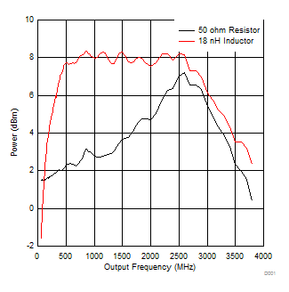
OUTx_PWR=15 | 7.3 | dBm | ||||
| OUTx_PWR=45 | 12 | ||||||||
| H2RFoutX+/- | Second Harmonic (6) |
Fout = 2.7 GHz | OUTx_PWR=15 | –25 | dBc | ||||
| VCO | |||||||||
| fVCO | Before the VCO Divider | All VCO Cores Combined | 1880 | 3760 | |||||
| KVCO | VCO Gain | Vtune = 1.3 Volts |
Core 1 | 12 to 24 | MHz/V | ||||
| Core 2 | 15 to 30 | ||||||||
| Core 3 | 20 to 37 | ||||||||
| Core 4 | 21 to 37 | ||||||||
| ΔTCL | Allowable Temperature Drift (3) |
VCO not being recalibrated | Fvco ≥2.5 GHz | –125 | +125 | °C | |||
| Fvco < 2.5 GHz | –100 | +125 | |||||||
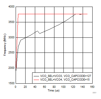
| tVCOCal | VCO Calibration Time (4) |
fOSCin = 100 MHz fPD = 100 MHz Full Band Change 1880 — 3760 MHz |
No Pre-programming | 140 | us | ||||
| With Pre-programming | 10 | ||||||||
| PNVCO | VCO Phase Noise (OUTx_PWR =15) |
fVCO = 1.9 GHz Core 1 |
10 kHz Offset | –85.4 | dBc /Hz | ||||
| 100 kHz Offset | –114.5 | ||||||||
| 1 MHz Offset | –137.0 | ||||||||
| 10 MHz Offset | –154.2 | ||||||||
| 40 MHz Offset | –156.7 | ||||||||
| fVCO = 2.2 GHz Core 2 |
10 kHz Offset | –84.6 | dBc /Hz | ||||||
| 100 kHz Offset | –114.1 | ||||||||
| 1 MHz Offset | –137.5 | ||||||||
| 10 MHz Offset | –154.5 | ||||||||
| 40 MHz Offset | –156.1 | ||||||||
| fVCO = 2.7 GHz Core 3 |
10 kHz Offset | –81.7 | dBc /Hz | ||||||
| 100 kHz Offset | –112.2 | ||||||||
| 1 MHz Offset | –136.0 | ||||||||
| 10 MHz Offset | –153.1 | ||||||||
| 40 MHz Offset | –155.0 | ||||||||
| fVCO = 3.3 GHz Core 4 |
10 kHz Offset | –79.0 | dBc /Hz | ||||||
| 100 kHz Offset | –108.6 | ||||||||
| 1 MHz Offset | –132.6 | ||||||||
| 10 MHz Offset | –152.0 | ||||||||
| 40 MHz Offset | –155.0 | ||||||||
| DIGITAL INTERFACE (DATA, CLK, LE, CE, MUXout, BUFEN, LD) | |||||||||
| VIH | High-Level Input Voltage | 1.4 | Vcc | V | |||||
| VIL | Low Level Input Voltage | 0.4 | V | ||||||
| IIH | High-Level Input Current | VIH = 1.75 V | –5 | 5 | µA | ||||
| IIL | Low-Level Input Current | VIL = 0 V | –5 | 5 | µA | ||||
| VOH | High-Level Output Voltage | IOH = -500 µA | 2 | V | |||||
| VOL | Low-Level Output Voltage | IOL = -500 µA | 0 | 0.4 | V | ||||
7.6 Timing Requirements, MICROWIRE Timing
| MIN | TYP | MAX | UNIT | |||
|---|---|---|---|---|---|---|
| tES | Clock to Enable Low Time | See Figure 1 | 35 | ns | ||
| tCS | Data to Clock Set Up Time | See Figure 1 | 10 | ns | ||
| tCH | Data to Clock Hold Time | See Figure 1 | 10 | ns | ||
| tCWH | Clock Pulse Width High | See Figure 1 | 25 | ns | ||
| tCWL | Clock Pulse Width Low | See Figure 1 | 25 | ns | ||
| tCES | Enable to Clock Set Up Time | See Figure 1 | 10 | ns | ||
| tEWH | Enable Pulse Width High | See Figure 1 | 10 | ns |
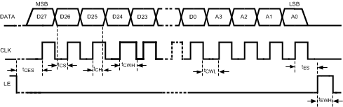 Figure 1. Serial Data Input Timing
7.7 Typical Characteristics