SLVAFA6 March 2022 LM74700-Q1 , TLV4041 , TPS272C45
1 Application Brief
Test pulses in digital output modules refer to a forced switching of a high-side switch (HSS) to the opposite level for a short time to verify the functionality of the output. This is particularly important for functional safety applications if the output state rarely changes. The off-test pulse applies if the switch is normally on (load energized). The on-test pulse applies if the switch is normally off (load de-energized). The connected load must not be influenced by this test. In off-test, the voltage at the HSS must drop to verify the correct function. A reverse current blocking is required to prevent any current from the load back to the HSS, which is essential to keep the load energized during the test. In on-test, a high output of the HSS allows for shorter charge time of the capacitive part of the load to verify the correct function of the HSS.
Implementation options
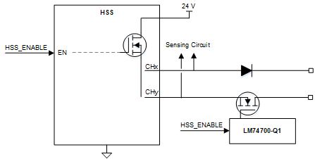
The reverse current blocking can be accomplished in different ways. The simplest way is adding a diode to the output (see Figure 1-1, CHx). The drawback of this approach is the power dissipation of the diode in on-state, which is dependent on the channel output current and the diode voltage drop.
A less power-dissipative solution can be created with the use of an NMOS and a smart diode controller, like the LM74700-Q1 (Figure 1-1, CHy). The LM74700-Q1 can block reverse-current autonomously, but also features a enable pin. As the HSS control signal is available (HSS_ENABLE) the LM74700-Q1 is controlled directly, effectively working as a NMOS gate driver.
 Figure 1-1 Implementation Options
Schematics discussion
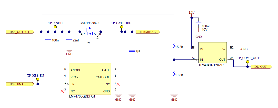
Figure 1-2 shows the schematics of an example circuit for reverse blocking using the LM74700-Q1. The HSS used for the test is the TPS272C45. An off-test is initiated by disabling the HSS output (signal HSS_OUTPUT) by pulling signal HSS_ENABLE low. The same signal is also used to turn off the LM74700-Q1.
The HSS_OUTPUT voltage node (test point TP_ANODE) is monitored by the comparator TLV4041R1(3). The 1.2-V reference integrated in the TLV4041R1 reduces BOM and board space. The resistor divider sets the comparator trip point to 12 V and provides a ground reference to the floating node when the output is disabled. The relatively low resistor divider helps to discharge the capacitors at the anode (HSS output) to allow short test pulses. The output of the comparator is either fed directly back to the controller or serialized first to reduce the number of isolated channels in an isolated application (see the Converting SPI to GPIO Through Digital Isolators application brief).
 Figure 1-2 Schematics of Implementation With LM74700-Q1
Test results
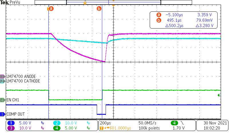
Figure 1-3 shows the relevant waveforms for the off-test with a 50 Ω||100-μF load. Waveform EN CH1 equals HSS_ENABLE and controls the HSS and the LM74700-Q1 enable pin. A test pulse length of 500 μs is sufficient to drop the HSS output voltage (waveform LM74700 ANODE) below 12 V to trip the comparator (waveform COMP OUT). The voltage at the load drops by only about 4 V with this output configuration. In digital output modules the pulse length can be adjusted to allow a wide range of loads.
 Figure 1-3 Off-Test Waveforms
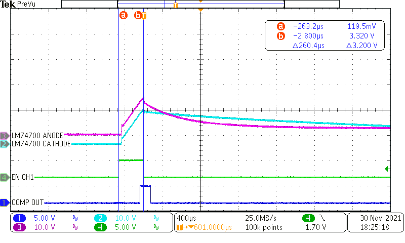
Figure 1-4 shows the relevant waveforms for the on-test with a 50 Ω||100-μF load and an HSS current limit of 2 A. However, the actual current is 4 A as the HSS output current is doubled for a selectable time (here 22 ms) to address capacitive loads(5), effectively shorten the pulse time. For this HSS-load configuration an HSS enable time of 260 μs is sufficient to trip the comparator with a threshold of 12 V.
The same comparator may be used if the off-test and on-test agree on the same voltage threshold. Note the inversion of the pulse relative to the off-test. The load should not turn on by the on-test pulse.
 Figure 1-4 On-Test Waveforms
Additional use-cases
In addition, the presented feature effectively blocks reverse current from the output terminals into the module if the voltage at the terminal exceeds the HSS supply voltage while the HSS is disabled. This can apply in the following scenarios:
- Universal digital I/O application where a terminal can be software-programmed as either digital input or digital output. In digital input configuration the voltage from the connected sensor may exceed the voltage of the HSS supply voltage causing a current into the module without the feature
- During a mis-wiring event, for example if a power supply is accidentally connected to an output terminal.
Conclusion
The off and on test is an effective means to verify correct operation of a digital output. Different methods exist to implement this feature. However, this implementation also supports universal I/O modules and protects against mis-wiring.
References
- LM74700-Q1 product folder
- TPS272C45 product folder
- TLV4041R1 product folder
- Texas Instruments, Converting SPI to GPIO Through Digital Isolators application brief
- Texas Instruments, How to Drive Resistive, Inductive, Capacitive, and Lighting Loads application report