-
bq27530-G1 Battery Management Unit Impedance Track™ Fuel Gauge with MaxLife Technology for Use with the bq2416x Charger Controller
- 1 Features
- 2 Applications
- 3 Description
- 4 Revision History
- 5 Pin Configuration and Functions
-
6 Specifications
- 6.1 Absolute Maximum Ratings
- 6.2 ESD Ratings
- 6.3 Thermal Information
- 6.4 Recommended Operating Conditions
- 6.5 Supply Current
- 6.6 Digital Input and Output DC Characteristics
- 6.7 Power-on Reset
- 6.8 2.5-V LDO Regulator
- 6.9 Internal Clock Oscillators
- 6.10 ADC (Temperature and Cell Measurement) Characteristics
- 6.11 Integrating ADC (Coulomb Counter) Characteristics
- 6.12 Data Flash Memory Characteristics
- 6.13 I2C-Compatible Interface Communication Timing Characteristics
- 6.14 Typical Characteristics
- 7 Detailed Description
- 8 Application and Implementation
- 9 Power Supply Recommendations
- 10Layout
- 11Device and Documentation Support
- 12Mechanical, Packaging, and Orderable Information
- IMPORTANT NOTICE
bq27530-G1 Battery Management Unit Impedance Track™ Fuel Gauge with MaxLife Technology for Use with the bq2416x Charger Controller
1 Features
- Battery Fuel Gauge and Charger Controller for 1-Cell Li-Ion Applications
- Resides on System Main Board
- Battery Fuel Gauge Based on Patented Impedance
Track™ Technology
- Models the Battery Discharge Curve for Accurate Time-to-Empty Predictions
- Automatically Adjusts for Battery Aging, Battery Self-Discharge, and Temperature/Rate Inefficiencies
- Low-Value Sense Resistor (5 mΩ to 20 mΩ)
- Battery Charger Controller with Customizable Charge Profiles
- Configurable Charge Voltage and Current based on Temperature
- Optional State-Of-Health (SOH) and Multi-Level Based Charge Profiles
- Host Free Autonomous Battery Management System
- Reduced Software Overhead Allows for Easy Portability Across Platforms and Shorter OEM Design Cycles
- Higher Safety and Security
- Run Time Improvements
- Longer Battery Runtime Leveraging Impedance Track Technology
- Tighter Accuracy Controls for Charger Termination
- Improved Recharged Thresholds
- Intelligent Charging—Customized and Adaptive Charging Profiles
- Charger Control Based on SOH
- Temperature Level Charging (TLC)
- Battery Charger Controller for bq2416x Single Cell Switchmode Battery Charger
- Stand-Alone Charging Solution
- 400-kHz I2C™ Interface for Connection to System Microcontroller Port
- In a 15-Pin NanoFree™ Packaging
2 Applications
- Smartphones, Feature Phones, and Tablets
- Digital Still and Video Cameras
- Handheld Terminals
- MP3 or Multimedia Players
3 Description
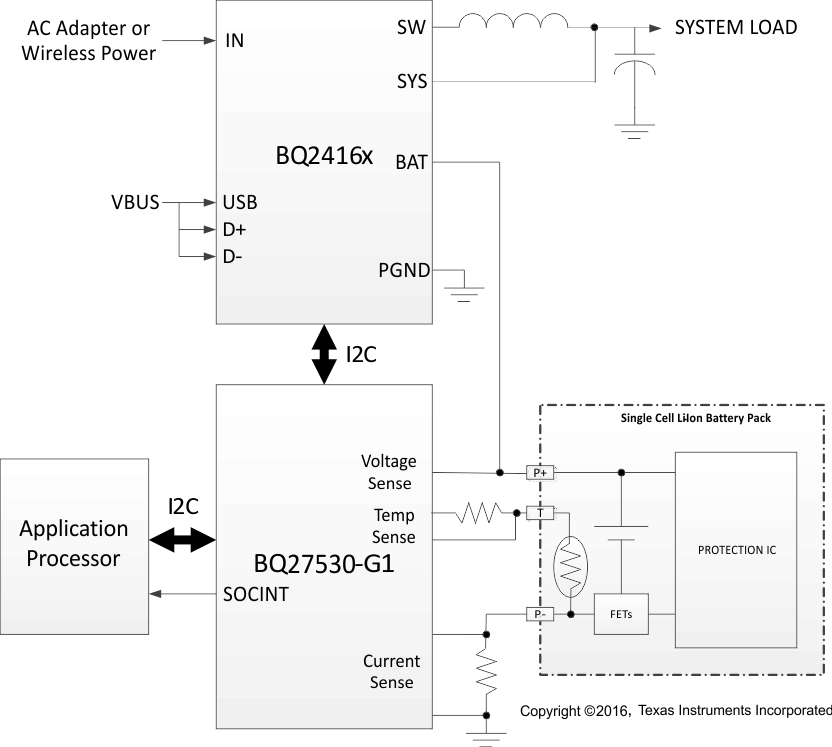
The Texas Instruments bq27530-G1 system-side Li-Ion Battery Management Unit is a microcontroller peripheral that provides Impedance Track™ fuel gauging and charging control for single-cell Li-Ion battery packs. The device requires little system microcontroller firmware development. Together with bq2416x Single-Cell Switchmode Charger, the bq27530-G1 manages an embedded battery (non-removable) or a removable battery pack.
The bq27530-G1 uses the patented Impedance Track™ algorithm for fuel gauging, and provides information such as remaining battery capacity (mAh), state-of-charge (%), runtime-to-empty (min), battery voltage (mV), temperature (°C), and state-of-health (%).
Device Information(1)
| PART NUMBER | PACKAGE | BODY SIZE (NOM) |
|---|---|---|
| bq27530-G1 | DSBGA (15) | 2.61 mm × 1.96 mm |
- For all available packages, see the orderable addendum at the end of the data sheet.
Simplified Schematic
4 Revision History
Changes from B Revision (January 2016) to C Revision
Changes from A Revision (May 2015) to B Revision
- Changed ESD Ratings Go
Changes from * Revision (December 2012) to A Revision
- Changed the data sheet title From: Battery Management Unit Impedance Track™ Fuel Gauge for Use With the bq2416x Charger Controller To: Battery Management Unit Impedance Track™ Fuel Gauge with MaxLife Technology for Use With the bq2416x Charger ControllerGo
- Added the ESD Ratings table, Detailed Description section, Feature Description section, Device Functional Modes section, Programming section, Application and Implementation section. Power Supply Recommendations section, Layout section, Device and Documentation Support section, Mechanical, Packaging, and Orderable Information sectionGo
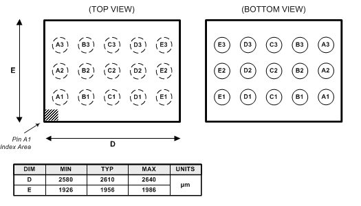
5 Pin Configuration and Functions
Pin Functions
| PIN | TYPE(1) | DESCRIPTION | |
|---|---|---|---|
| NAME | NO. | ||
| SRP | A1 | IA | Analog input pin connected to the internal coulomb counter where SRP is nearest the PACK– connection. Connect to 5-mΩ to 20-mΩ sense resistor. |
| SRN | B1 | IA | Analog input pin connected to the internal coulomb counter where SRN is nearest the Vss connection. Connect to 5-mΩ to 20-mΩ sense resistor. |
| VSS | C1, C2 | P | Device ground |
| VCC | D1 | P | Regulator output and bq27530-G1 power. Decouple with 1μF ceramic capacitor to Vss. |
| REGIN | E1 | P | Regulator input. Decouple with 0.1-μF ceramic capacitor to Vss. |
| SOC_INT | A2 | I/O | SOC state interrupts output. Open drain output. |
| BSCL | B2 | O | Battery Charger clock output line for chipset communication. Push-pull output. Note: CE has an internal ESD protection diode connected to REGIN. Recommend maintaining VCE ≤ VREGIN under all conditions. |
| CE | D2 | I | Chip Enable. Internal LDO is disconnected from REGIN when driven low. |
| BAT | E2 | I | Cell-voltage measurement input. ADC input. Recommend 4.8V maximum for conversion accuracy. |
| SCL | A3 | I | Slave I2C serial communications clock input line for communication with system (Master). Open-drain I/O. Use with 10kΩ pull-up resistor (typical). |
| SDA | B3 | I/O | Slave I2C serial communications data line for communication with system (Master). Open-drain I/O. Use with 10kΩ pull-up resistor (typical). |
| BSDA | C3 | I/O | Battery Charger data line for chipset communication. Push-pull output. |
| TS | D3 | IA | Pack thermistor voltage sense (use 103AT-type thermistor). ADC input. |
| BI/TOUT | E3 | I/O | Battery-insertion detection input. Power pin for pack thermistor network. Thermistor-multiplexer control pin. Use with pull-up resistor >1MΩ (1.8 MΩ typical). |
6 Specifications
6.1 Absolute Maximum Ratings
over operating free-air temperature range (unless otherwise noted)(1)| MIN | MAX | UNIT | ||
|---|---|---|---|---|
| VREGIN | Regulator input range | –0.3 to 5.5 | 5.5 | V |
| –0.3 | 6 (2) | V | ||
| VCE | CE input pin | –0.3 | VREGIN + 0.3 | V |
| VCC | Supply voltage range | –0.3 | 2.75 | V |
| VIOD | Open-drain I/O pins (SDA, SCL, SOC_INT) | –0.3 | 5.5 | V |
| VBAT | BAT input pin | –0.3 | 5.5 | V |
| –0.3 | 6 (2) | V | ||
| VI | Input voltage range to all other pins (BI/TOUT, TS, SRP, SRN, BSDA, BSCL) |
–0.3 | VCC + 0.3 | V |
| TA | Operating free-air temperature range | –40 | 85 | °C |
| Tstg | Storage temperature range | –65 | 150 | °C |
6.2 ESD Ratings
| VALUE | UNIT | |||
|---|---|---|---|---|
| V(ESD) | Electrostatic discharge | Human-body model (HBM), per ANSI/ESDA/JEDEC JS-001, BAT pin(1) | ±1500 | V |
| Human-body model (HBM), per ANSI/ESDA/JEDEC JS-001, All other pins(1) | ±2000 | |||
| Charged device model(CDM), per JEDEC specification JESD22-C101(2) | ±250 | |||
6.3 Thermal Information
| THERMAL METRIC(1) | bq27530-G1 | UNIT | |
|---|---|---|---|
| YZF (DSBGA) | |||
| 15 PINS | |||
| RθJA | Junction-to-ambient thermal resistance | 70 | °C/W |
| RθJC(top) | Junction-to-case (top) thermal resistance | 17 | °C/W |
| RθJB | Junction-to-board thermal resistance | 20 | °C/W |
| ψJT | Junction-to-top characterization parameter | 1 | °C/W |
| ψJB | Junction-to-board characterization parameter | 18 | °C/W |
| RθJC(bot) | Junction-to-case (bottom) thermal resistance | n/a | °C/W |
6.4 Recommended Operating Conditions
TA = –40°C to 85°C, VREGIN = VBAT = 3.6 V (unless otherwise noted)| PARAMETER | TEST CONDITIONS | MIN | NOM | MAX | UNIT | |
|---|---|---|---|---|---|---|
| VREGIN | Supply voltage | No operating restrictions | 2.8 | 4.5 | V | |
| No flash writes | 2.45 | 2.8 | ||||
| CREGIN | External input capacitor for internal LDO between REGIN and VSS | Nominal capacitor values specified. Recommend a 5% ceramic X5R type capacitor located close to the device. | 0.1 | μF | ||
| CLDO25 | External output capacitor for internal LDO between VCC and VSS | 0.47 | 1 | μF | ||
| tPUCD | Power-up communication delay | 250 | ms | |||
6.5 Supply Current
TA = 25°C and VREGIN = VBAT = 3.6 V (unless otherwise noted)| PARAMETER | TEST CONDITIONS | MIN | TYP | MAX | UNIT | |
|---|---|---|---|---|---|---|
| ICC (1) | Normal operating-mode current | Fuel gauge in NORMAL mode ILOAD > Sleep current |
118 | μA | ||
| ISLP+ (1) | Sleep+ operating mode current | Fuel gauge in SLEEP+ mode ILOAD < Sleep current |
62 | μA | ||
| ISLP (1) | Low-power storage-mode current | Fuel gauge in SLEEP mode ILOAD < Sleep current |
23 | μA | ||
| IHIB (1) | Hibernate operating-mode current | Fuel gauge in HIBERNATE mode ILOAD < Hibernate current |
8 | μA | ||
6.6 Digital Input and Output DC Characteristics
TA = –40°C to 85°C, typical values at TA = 25°C and VREGIN = 3.6 V (unless otherwise noted)| PARAMETER | TEST CONDITIONS | MIN | TYP | MAX | UNIT | |
|---|---|---|---|---|---|---|
| VOL | Output voltage, low (SCL, SDA, SOC_INT, BSDA, BSCL) | IOL = 3 mA | 0.4 | V | ||
| VOH(PP) | Output voltage, high (BSDA, BSCL) | IOH = –1 mA | VCC – 0.5 | V | ||
| VOH(OD) | Output voltage, high (SDA, SCL, SOC_INT) | External pullup resistor connected to VCC | VCC – 0.5 | |||
| VIL | Input voltage, low (SDA, SCL) | –0.3 | 0.6 | V | ||
| Input voltage, low (BI/TOUT) | BAT INSERT CHECK MODE active | –0.3 | 0.6 | |||
| VIH | Input voltage, high (SDA, SCL) | 1.2 | V | |||
| Input voltage, high (BI/TOUT) | BAT INSERT CHECK MODE active | 1.2 | VCC + 0.3 | |||
| VIL(CE) | Input voltage, low (CE) | VREGIN = 2.8 to 4.5V | 0.8 | V | ||
| VIH(CE) | Input voltage, high (CE) | 2.65 | ||||
| Ilkg (1) | Input leakage current (I/O pins) | 0.3 | μA | |||
6.7 Power-on Reset
TA = –40°C to 85°C, typical values at TA = 25°C and VREGIN = 3.6 V (unless otherwise noted)| PARAMETER | TEST CONDITIONS | MIN | TYP | MAX | UNIT | |
|---|---|---|---|---|---|---|
| VIT+ | Positive-going battery voltage input at VCC | 2.05 | 2.15 | 2.20 | V | |
| VHYS | Power-on reset hysteresis | 115 | mV | |||
6.8 2.5-V LDO Regulator
TA = –40°C to 85°C, CLDO25 = 1 μF, VREGIN = 3.6 V (unless otherwise noted)| PARAMETER | TEST CONDITIONS | MIN | TYP | MAX | UNIT | |
|---|---|---|---|---|---|---|
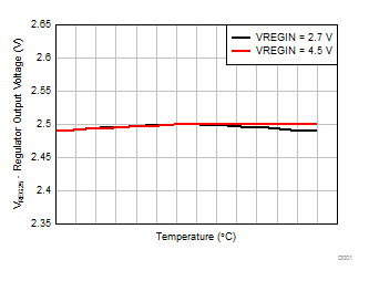
| VIREG25 | Regulator output voltage VCC | 2.8 V ≤ VREGIN ≤ 4.5 V, IOUT ≤ 16 mA(1) | 2.3 | 2.5 | 2.6 | V |
| 2.45 V ≤ VREGIN < 2.8 V (low battery), IOUT ≤ 3mA | 2.3 | V | ||||
6.9 Internal Clock Oscillators
TA = –40°C to 85°C, 2.4 V < VCC < 2.6 V; typical values at TA = 25°C and VCC = 2.5 V (unless otherwise noted)| PARAMETER | TEST CONDITIONS | MIN | TYP | MAX | UNIT | |
|---|---|---|---|---|---|---|
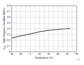
| fOSC | High frequency oscillator | 8.389 | MHz | |||
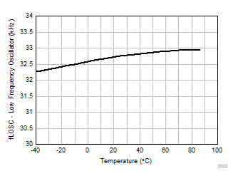
| fLOSC | Low frequency oscillator | 32.768 | kHz | |||
6.10 ADC (Temperature and Cell Measurement) Characteristics
TA = –40°C to 85°C, 2.4 V < VCC < 2.6 V; typical values at TA = 25°C and VCC = 2.5 V (unless otherwise noted)| PARAMETER | TEST CONDITIONS | MIN | TYP | MAX | UNIT | |
|---|---|---|---|---|---|---|
| VADC1 | Input voltage range (TS) | VSS – 0.125 | 2 | V | ||
| VADC2 | Input voltage range (BAT) | VSS – 0.125 | 5 | V | ||
| VIN(ADC) | Input voltage range | 0.05 | 1 | V | ||
| GTEMP | Internal temperature sensor voltage gain | –2 | mV/°C | |||
| tADC_CONV | Conversion time | 125 | ms | |||
| Resolution | 14 | 15 | bits | |||
| VOS(ADC) | Input offset | 1 | mV | |||
| ZADC1 (1) | Effective input resistance (TS) | 8 | MΩ | |||
| ZADC2 (1) | Effective input resistance (BAT) | bq27530-G1 not measuring cell voltage | 8 | MΩ | ||
| bq27530-G1 measuring cell voltage | 100 | kΩ | ||||
| Ilkg(ADC) (1) | Input leakage current | 0.3 | μA | |||
6.11 Integrating ADC (Coulomb Counter) Characteristics
TA = –40°C to 85°C, 2.4 V < VCC < 2.6 V; typical values at TA = 25°C and VCC = 2.5 V (unless otherwise noted)| PARAMETER | TEST CONDITIONS | MIN | TYP | MAX | UNIT | |
|---|---|---|---|---|---|---|
| VSR | Input voltage range, V(SRP) and V(SRN) |
VSR = V(SRP) – V(SRN) | –0.125 | 0.125 | V | |
| tSR_CONV | Conversion time | Single conversion | 1 | s | ||
| Resolution | 14 | 15 | bits | |||
| VOS(SR) | Input offset | 10 | μV | |||
| INL | Integral nonlinearity error | ±0.007% | ±0.034% | FSR | ||
| ZIN(SR) (1) | Effective input resistance | 2.5 | MΩ | |||
| Ilkg(SR)(1) | Input leakage current | 0.3 | μA | |||
6.12 Data Flash Memory Characteristics
TA = –40°C to 85°C, 2.4 V < VCC < 2.6 V; typical values at TA = 25°C and VCC = 2.5 V (unless otherwise noted)| PARAMETER | TEST CONDITIONS | MIN | TYP | MAX | UNIT | |
|---|---|---|---|---|---|---|
| tDR (1) | Data retention | 10 | Years | |||
| Flash-programming write cycles(1) | 20,000 | Cycles | ||||
| tWORDPROG (1) | Word programming time | 2 | ms | |||
| ICCPROG (1) | Flash-write supply current | 5 | 10 | mA | ||
| tDFERASE (1) | Data flash master erase time | 200 | ms | |||
| tIFERASE (1) | Instruction flash master erase time | 200 | ms | |||
| tPGERASE (1) | Flash page erase time | 20 | ms | |||
6.13 I2C-Compatible Interface Communication Timing Characteristics
TA = –40°C to 85°C, 2.4 V < VCC < 2.6 V; typical values at TA = 25°C and VCC = 2.5 V (unless otherwise noted)| MIN | NOM | MAX | UNIT | ||
|---|---|---|---|---|---|
| tr | SCL/SDA rise time | 300 | ns | ||
| tf | SCL/SDA fall time | 300 | ns | ||
| tw(H) | SCL pulse duration (high) | 600 | ns | ||
| tw(L) | SCL pulse duration (low) | 1.3 | μs | ||
| tsu(STA) | Setup for repeated start | 600 | ns | ||
| td(STA) | Start to first falling edge of SCL | 600 | ns | ||
| tsu(DAT) | Data setup time | 100 | ns | ||
| th(DAT) | Data hold time | 0 | ns | ||
| tsu(STOP) | Setup time for stop | 600 | ns | ||
| t(BUF) | Bus free time between stop and start | 66 | μs | ||
| fSCL | Clock frequency (1) | 400 | kHz | ||
 Figure 1. I2C-compatible Interface Timing Diagrams
6.14 Typical Characteristics
