-
CSD18563Q5A 60 V N-Channel NexFET™ Power MOSFET
CSD18563Q5A 60 V N-Channel NexFET™ Power MOSFET
1 Features
2 Applications
3 Description
This 5.7 mΩ, 60 V SON 5 mm × 6 mm NexFET™ power MOSFET was designed to pair with the CSD18537NQ5A control FET and act as the sync FET for a complete industrial buck converter chipset solution.
Product Summary
| TA = 25°C | TYPICAL VALUE | UNIT | ||
|---|---|---|---|---|
| VDS | Drain-to-Source Voltage | 60 | V | |
| Qg | Gate Charge Total (10 V) | 15.0 | nC | |
| Qgd | Gate Charge Gate-to-Drain | 2.9 | nC | |
| RDS(on) | Drain-to-Source On-Resistance | VGS = 4.5 V | 8.6 | mΩ |
| VGS = 10 V | 5.7 | mΩ | ||
| VGS(th) | Threshold Voltage | 2.0 | V | |
.
Ordering Information(1)
| DEVICE | MEDIA | QTY | PACKAGE | SHIP |
|---|---|---|---|---|
| CSD18563Q5A | 13-Inch Reel | 2500 | SON 5 × 6 mm Plastic Package |
Tape and Reel |
| CSD18563Q5AT | 7-Inch Reel | 250 |
- For all available packages, see the orderable addendum at the end of the data sheet.
Absolute Maximum Ratings
| TA = 25°C | VALUE | UNIT | |
|---|---|---|---|
| VDS | Drain-to-Source Voltage | 60 | V |
| VGS | Gate-to-Source Voltage | ±20 | V |
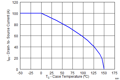
| ID | Continuous Drain Current (Package limited) | 100 | A |
| Continuous Drain Current (Silicon limited), TC = 25°C | 93 | ||
| Continuous Drain Current(1) | 15 | ||
| IDM | Pulsed Drain Current(2) | 251 | A |
| PD | Power Dissipation(1) | 3.2 | W |
| Power Dissipation, TC = 25°C | 116 | ||
| TJ, Tstg |
Operating Junction Temperature, Storage Temperature |
–55 to 150 | °C |
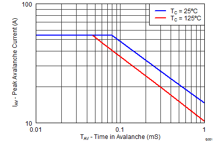
| EAS | Avalanche Energy, single pulse ID = 54 A, L = 0.1 mH, RG = 25 Ω |
146 | mJ |
RDS(on) vs VGS |
Gate Charge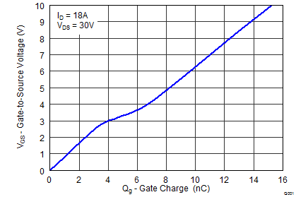 |
4 Revision History
Changes from B Revision (January 2015) to C Revision
- Added "Soft Body Diode for Reduced Ringing" under Features Go
- Added "Low-Side FET for Industrial Buck Converter" to ApplicationsGo
- Updated the part description Go
- Added the Community Resources sectionGo
Changes from A Revision (January 2014) to B Revision
- Increased silicon limited continuous drain current to 93 A Go
- Increased Pulsed Drain Current to 251 Go
- Added line for max power dissipation with case temperature held to 25° CGo
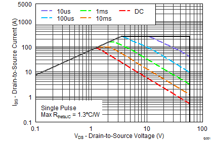
- Updated pulsed current conditions Go
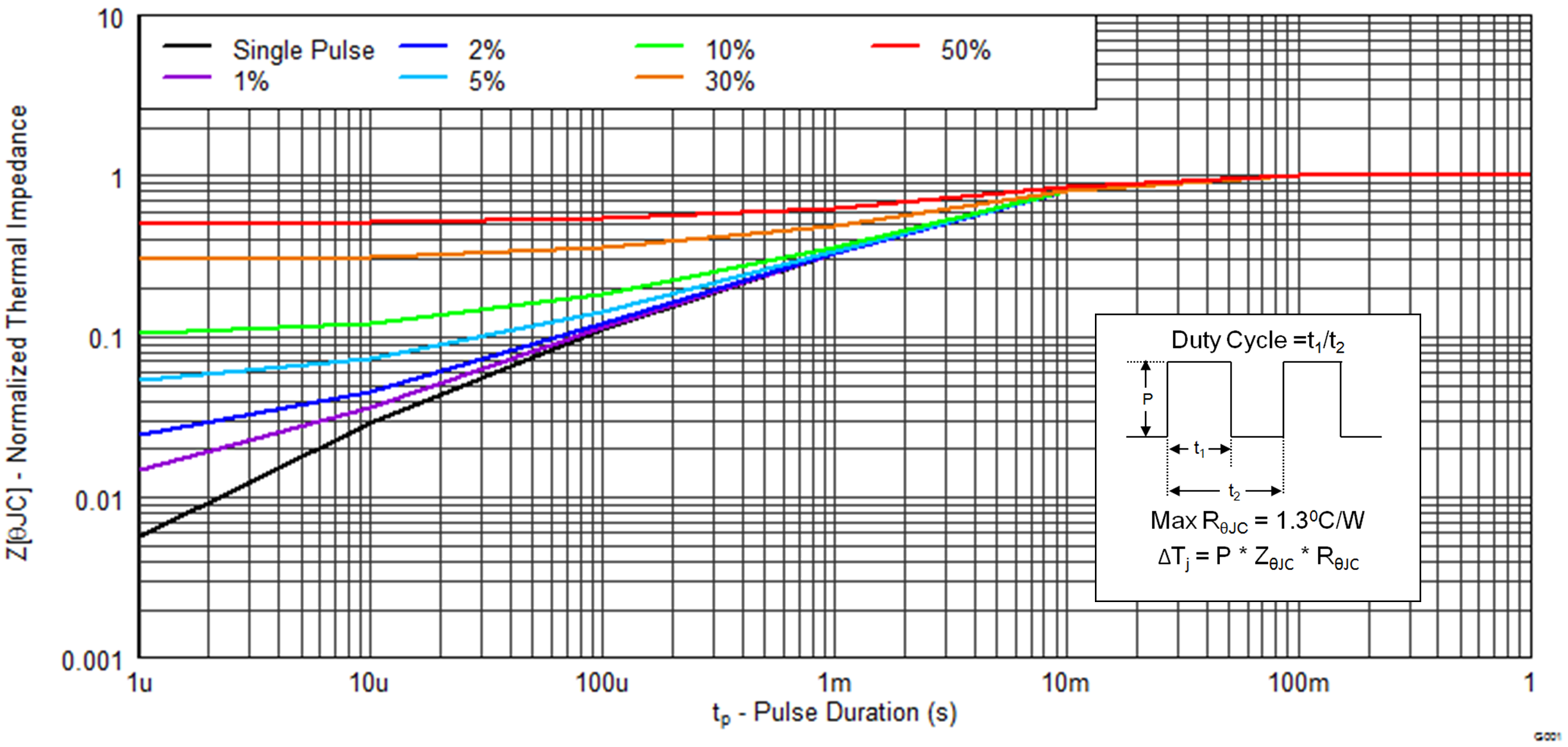
- Changed Figure 1 to normalized RθJC curve Go
- Updated SOA in Figure 10 Go
Changes from * Revision (July 2013) to A Revision
5 Specifications
5.1 Electrical Characteristics
(TA = 25°C unless otherwise stated)| PARAMETER | TEST CONDITIONS | MIN | TYP | MAX | UNIT | ||
|---|---|---|---|---|---|---|---|
| STATIC CHARACTERISTICS | |||||||
| BVDSS | Drain-to-source voltage | VGS = 0 V, ID = 250 μA | 60 | V | |||
| IDSS | Drain-to-source leakage current | VGS = 0 V, VDS = 48 V | 1 | μA | |||
| IGSS | Gate-to-source leakage current | VDS = 0 V, VGS = 20 V | 100 | nA | |||
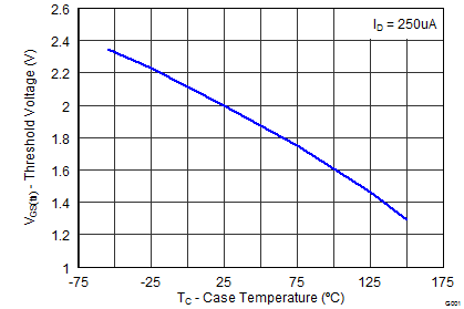
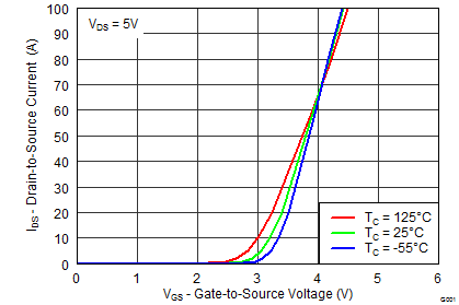
| VGS(th) | Gate-to-source threshold voltage | VDS = VGS, ID = 250 μA | 1.7 | 2.0 | 2.4 | V | |
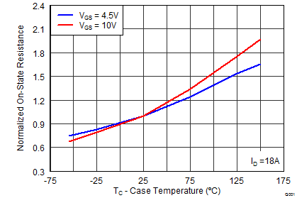
| RDS(on) | Drain-to-source on resistance | VGS = 4.5 V, ID = 18 A | 8.6 | 10.8 | mΩ | ||
| VGS = 10 V, ID = 18 A | 5.7 | 6.8 | mΩ | ||||
| gfs | Transconductance | VDS = 30 V, ID = 18 A | 60 | S | |||
| DYNAMIC CHARACTERISTICS | |||||||
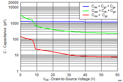
| Ciss | Input capacitance | VGS = 0 V, VDS = 30 V, ƒ = 1 MHz | 1150 | 1500 | pF | ||
| Coss | Output capacitance | 280 | 364 | pF | |||
| Crss | Reverse transfer capacitance | 3.9 | 5.1 | pF | |||
| RG | Series gate resistance | 1.5 | 3.0 | Ω | |||
| Qg | Gate charge total (4.5 V) | VDS = 30 V, ID = 18 A | 7.3 | 9.5 | nC | ||
| Qg | Gate charge total (10 V) | 15 | 20 | ||||
| Qgd | Gate charge gate-to-drain | 2.9 | nC | ||||
| Qgs | Gate charge gate-to-source | 3.3 | nC | ||||
| Qg(th) | Gate charge at Vth | 2.3 | nC | ||||
| Qoss | Output charge | VDS = 30 V, VGS = 0 V | 36 | nC | |||
| td(on) | Turn on delay time | VDS = 30 V, VGS = 10 V, IDS = 18 A, RG = 0 Ω | 3.2 | ns | |||
| tr | Rise time | 6.3 | ns | ||||
| td(off) | Turn off delay time | 11.4 | ns | ||||
| tf | Fall time | 1.7 | ns | ||||
| DIODE CHARACTERISTICS | |||||||
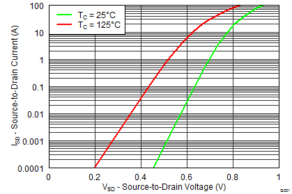
| VSD | Diode forward voltage | ISD = 18 A, VGS = 0 V | 0.8 | 1 | V | ||
| Qrr | Reverse recovery charge | VDS= 30 V, IF = 18 A, di/dt = 300 A/μs | 63 | nC | |||
| trr | Reverse recovery time | 49 | ns | ||||
5.2 Thermal Information
(TA = 25°C unless otherwise stated)| THERMAL METRIC | MIN | TYP | MAX | UNIT | |
|---|---|---|---|---|---|
| RθJC | Junction-to-case thermal resistance(1) | 1.3 | °C/W | ||
| RθJA | Junction-to-ambient thermal resistance(1)(2) | 50 | |||
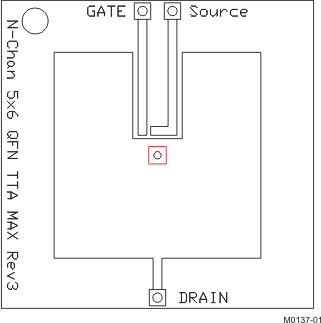 |
Max RθJA = 50°C/W when mounted on 1 inch2 (6.45 cm2) of 2 oz. (0.071 mm thick) Cu. |
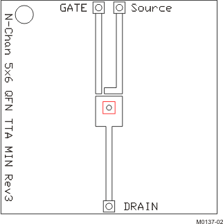 |
Max RθJA = 125°C/W when mounted on a minimum pad area of 2 oz. (0.071 mm thick) Cu. |
5.3 Typical MOSFET Characteristics
(TA = 25°C unless otherwise stated)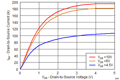


6 Device and Documentation Support
6.1 Community Resources
The following links connect to TI community resources. Linked contents are provided "AS IS" by the respective contributors. They do not constitute TI specifications and do not necessarily reflect TI's views; see TI's Terms of Use.
-
TI E2E™ Online Community TI's Engineer-to-Engineer (E2E) Community. Created to foster collaboration among engineers. At e2e.ti.com, you can ask questions, share knowledge, explore ideas and help solve problems with fellow engineers.
-
Design Support TI's Design Support Quickly find helpful E2E forums along with design support tools and contact information for technical support.
6.2 Trademarks
NexFET, E2E are trademarks of Texas Instruments.
All other trademarks are the property of their respective owners.
6.3 Electrostatic Discharge Caution

These devices have limited built-in ESD protection. The leads should be shorted together or the device placed in conductive foam during storage or handling to prevent electrostatic damage to the MOS gates.
6.4 Glossary
SLYZ022 — TI Glossary.
This glossary lists and explains terms, acronyms, and definitions.
