SCLA050 November 2021 SN74HCS08
1
Functional Block Diagram
Simplified Block Diagram for Single Board Computers shows a simplified single board computer block diagram to illustrate the logic and translation use cases. Each red block has an associated use-case document. Links are provided in Table 1-1 and Table 1-2. For a more complete block diagram, see the interactive online end equipment reference diagram for single board computers.
Logic and Translation Use Cases
Each use case links to a separate document that provides additional details including a block diagram, design tips, and part recommendations. The nearest block and use-case identifiers are listed to match up exactly to the use cases shown in the provided simplified block diagram.
| Nearest Block | Use-Case Identifier | Use Case |
|---|---|---|
| Point-of-Load Regulators | Power Good Combination | Combine Power Good Signals |
| Housekeeping | Fault Combination | Use Fewer Inputs to Monitor Error Signals |
| User Interface | Indicator LED | Drive Indicator LEDs |
| Output Expansion | Increase the Number of Outputs on a Microcontroller | |
| Clocking | Buffer | Redrive Digital Signals |
| Nearest Block | Use-Case Identifier | Use Case |
|---|---|---|
| Network Interface | RGMII | Translate Voltages for RGMII |
| MDIO | Translate Voltages for MDIO | |
| Input/Output Interface | SPI | Translate Voltages for SPI |
| I2C | Voltage Translation for I2C Interface Modules | |
| GPIO | Translate Voltages for GPIO |
Voltage Translation for I2C Interface Modules
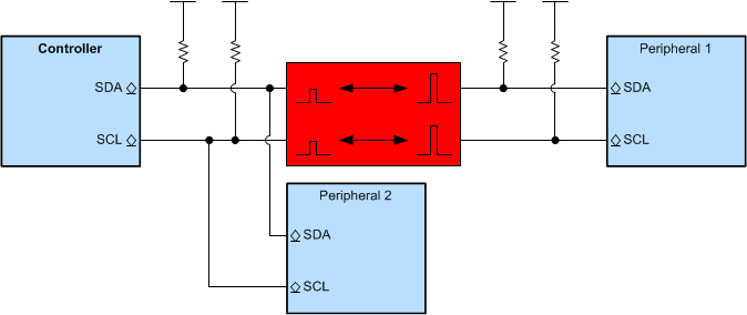
It is common to see single board computers providing at least one I2C interface to connect external sensors or other modules. These external components can operate at a different voltage than the primary system controller. The addition of a voltage level translator protects low-power system controllers and ensures accurate communication to the peripheral module.
 Figure 1-2 Example I2C Voltage
Translation Block Diagram
Figure 1-2 Example I2C Voltage
Translation Block Diagram- Typically operates at 100 kbps, 400 kbps, or 3.4 Mbps
- Requires auto-bidirectional, open-drain compatible voltage translators
- Translators enable communication when devices have mismatched logic voltage levels
- Prevents damage to devices that cannot support higher voltage inputs
- Improves data rates and signal integrity over discrete translation solutions
- Protects controller while peripheral is not connected
- Need additional assistance? Ask our engineers a question on the TI E2E™ Logic Support Forum
| Part Number | Automotive Qualified | Voltage Translation Range | Features |
|---|---|---|---|
| LSF0102-Q1 | ✓ | 0.95 V to 5.5 V to 0.95 V to 5.5 V |
Auto-bidirectional with open-drain
support Flexible design with external pull-up resistors See Understanding the LSF family of bidirectional, multi-voltage level translators for detailed design instructions |
| LSF0102 | |||
| TXS0102-Q1 | ✓ | 1.65 V to 3.6 V to 2.3 V to 5.5 V |
Auto-bidirectional with open-drain
support One-shot edge accelerators improve signal integrity Internal 10-kΩ pull-up resistors reduce external component count |
| TXS0102 | 1.2 V to 3.6 V to 1.65 V to 5.5 V |
For more I2C translation devices, browse through the online parametric tool where you can sort by desired voltage, channel numbers, and other features.