-
TMP708 Resistor-Programmable Temperature Switch in SOT Package
- 1 Features
- 2 Applications
- 3 Description
- 4 Revision History
- 5 Pin Configuration and Functions
- 6 Specifications
- 7 Detailed Description
- 8 Application and Implementation
- 9 Power Supply Recommendations
- 10Layout
- 11Device and Documentation Support
- 12Mechanical, Packaging, and Orderable Information
- IMPORTANT NOTICE
DATA SHEET
TMP708 Resistor-Programmable Temperature Switch in SOT Package
1 Features
-
Threshold Accuracy:
- ±0.5°C Typical
- ±3°C Maximum (60°C to 100°C)
- Temperature Threshold Set By 1% External Resistor
- Low Quiescent Current: 40 μA, Typical
- Open-Drain, Active-Low Output Stage
- Pin-Selectable 10°C or 30°C Hysteresis
- Reset Operation Specified at VCC = 0.8 V
- Supply Range: 2.7 V to 5.5 V
- Package: 5-Pin SOT-23
2 Applications
- Computers (Laptops and Desktops)
- Servers
- Industrial and Medical Equipment
- Storage Area Networks
- Automotive
3 Description
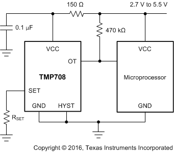
The TMP708 is a fully-integrated, resistor- programmable temperature switch with a temperature threshold that is set by just one external resistor within the entire operating range. The TMP708 provides an open-drain, active-low output and has a 2.7-V to 5.5-V supply voltage range.
The temperature threshold accuracy is typically ±0.5°C, with a maximum of ±3°C (60°C to 100°C). The quiescent current consumption is typically 40 μA. Hysteresis is pin-selectable to 10°C or 30°C.
The TMP708 is available in a 5-pin, SOT-23 package.
Device Information(1)
| PART NUMBER | PACKAGE | BODY SIZE (NOM) |
|---|---|---|
| TMP708 | SOT-23 (5) | 2.90 mm x 1.60 mm |
- For all available packages, see the package option addendum at the end of the datasheet.
Typical Application
4 Revision History
Changes from A Revision (February 2012) to B Revision
- Added Device Information, ESD Ratings, and Recommended Operating Conditions tables, and Detailed Description, Application and Implementation, Power Supply Recommendations, Layout, Device and Documentation Support, and Mechanical, Packaging, and Orderable Information sectionsGo
- Deleted Package and Ordering Information table; information now available in package option addendum located at the end of this data sheet Go
Changes from * Revision (December 2011) to A Revision
5 Pin Configuration and Functions
DBV Package
5-Pin SOT-23
Top View
Pin Functions
| PIN | TYPE | DESCRIPTION | |
|---|---|---|---|
| NAME | NO. | ||
| GND | 2 | Analog power | Device ground |
| HYST | 4 | Digital input | Hysteresis selection. For 10°C, HYST = VCC; for 30°C, HYST = GND. |
| OT | 3 | Digital output | Open-drain, active low output |
| SET | 1 | Analog input | Temperature set point. Connect an external 1% resistor between SET and GND. |
| VCC | 5 | Analog power | Power-supply voltage (2.7 V to 5.5 V) |
6 Specifications
6.1 Absolute Maximum Ratings
over operating free-air temperature range (unless otherwise noted) (1)| MIN | MAX | UNIT | ||
|---|---|---|---|---|
| Voltage | Supply, VCC | –0.3 | 6 | V |
| Input, SET and HYST | –0.3 | VCC + 0.3 | ||
| Output, OT | –0.3 | 6 | ||
| Current | Input | 20 | mA | |
| Output | 20 | |||
| Temperature | Operating, TA | –40 | 125 | °C |
| Junction, TJ | 150 | |||
| Storatge, Tstg | –65 | 150 |
(1) Stresses beyond those listed under Absolute Maximum Ratings may cause permanent damage to the device. These are stress ratings only, which do not imply functional operation of the device at these or any other conditions beyond those indicated under Recommended Operating Conditions. Exposure to absolute-maximum-rated conditions for extended periods may affect device reliability.
6.2 ESD Ratings
| VALUE | UNIT | |||
|---|---|---|---|---|
| V(ESD) | Electrostatic discharge | Human-body model (HBM), per ANSI/ESDA/JEDEC JS-001(1) | ±4000 | V |
| Charged-device model (CDM), per JEDEC specification JESD22-C101(2) | ±1000 | |||
| Machine model (MM) | ±200 | |||
(1) JEDEC document JEP155 states that 500-V HBM allows safe manufacturing with a standard ESD control process.
(2) JEDEC document JEP157 states that 250-V CDM allows safe manufacturing with a standard ESD control process.
6.3 Recommended Operating Conditions
over operating free-air temperature range (unless otherwise noted)| MIN | NOM | MAX | UNIT | ||
|---|---|---|---|---|---|
| VCC | Supply voltage | 2.7 | 5.5 | V | |
| TA | Operating temperature | 0 | 125 | °C | |
6.4 Thermal Information
| THERMAL METRIC(1) | TMP708 | UNIT | |
|---|---|---|---|
| DBV (SOT-23) | |||
| 5 PINS | |||
| RθJA | Junction-to-ambient thermal resistance | 217.9 | °C/W |
| RθJC(top) | Junction-to-case (top) thermal resistance | 86.3 | °C/W |
| RθJB | Junction-to-board thermal resistance | 44.6 | °C/W |
| ψJT | Junction-to-top characterization parameter | 4.4 | °C/W |
| ψJB | Junction-to-board characterization parameter | 43.8 | °C/W |
| RθJC(bot) | Junction-to-case (bottom) thermal resistance | N/A | °C/W |
(1) For more information about traditional and new thermal metrics, see the Semiconductor and IC Package Thermal Metrics application report.
6.5 Electrical Characteristics
at TA = 0°C to 125°C and VCC = 2.7 V to 5.5 V (unless otherwise noted)6.6 Typical Characteristics
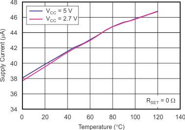
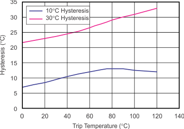
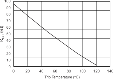
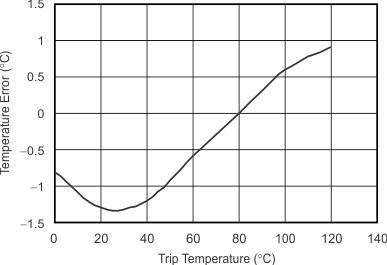
at TA = 25°C and VCC = 2.7 V to 5.5 V (unless otherwise noted)