SLPS506 August 2014 CSD23202W10
PRODUCTION DATA.
- 1Features
- 2Applications
- 3Description
- 4Revision History
- 5Specifications
- 6Device and Documentation Support
- 7Mechanical, Packaging, and Orderable Information
Package Options
Refer to the PDF data sheet for device specific package drawings
Mechanical Data (Package|Pins)
- YZB|4
Thermal pad, mechanical data (Package|Pins)
Orderable Information
1 Features
- Ultra-Low Qg and Qgd
- Small Footprint 1 mm × 1 mm
- Low Profile 0.62-mm Height
- Pb Free
- Gate ESD Protection – 3 kV
- RoHS Compliant
- Halogen Free
2 Applications
- Battery Management
- Load Switch
- Battery Protection
3 Description
This 12 V, 44 mΩ device is designed to deliver the lowest on-resistance and gate charge in a small
1 mm × 1 mm outline with excellent thermal characteristics in an ultra-low profile.
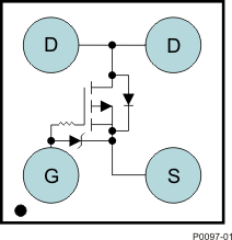
Top View
Product Summary
| TA = 25°C | TYPICAL VALUE | UNIT | ||
|---|---|---|---|---|
| VDS | Drain-to-Source Voltage | –12 | V | |
| Qg | Gate Charge Total (–4.5 V) | 2.9 | nC | |
| Qgd | Gate Charge Gate-to-Drain | 0.28 | nC | |
| RDS(on) | Drain-to-Source On-Resistance | VGS = –1.5 V | 82 | mΩ |
| VGS = –1.8 V | 67 | mΩ | ||
| VGS = –2.5 V | 54 | mΩ | ||
| VGS = –4.5 V | 44 | mΩ | ||
| VGS(th) | Threshold Voltage | –0.60 | V | |
Ordering Information(1)
| Device | Qty | Media | Package | Ship |
|---|---|---|---|---|
| CSD23202W10 | 3000 | 7-Inch Reel | 1 × 1-mm Wafer Level Package | Tape and Reel |
| CSD23202W10T | 250 | 7-Inch Reel |
- For all available packages, see the orderable addendum at the end of the data sheet.
Absolute Maximum Ratings
| TA = 25°C | VALUE | UNIT | |
|---|---|---|---|
| VDS | Drain-to-Source Voltage | –12 | V |
| VGS | Gate-to-Source Voltage | –6 | V |
| ID | Continuous Drain Current(1) | –2.2 | A |
| IDM | Pulsed Drain Current(2) | –25 | A |
| IG | Continuous Gate Clamp Current | –0.5 | A |
| Pulsed Gate Clamp Current | –7 | A | |
| PD | Power Dissipation(1) | 1 | W |
| TJ, Tstg |
Operating Junction and Storage Temperature Range |
–55 to 150 | °C |
- Device operating at a temperature of 105°C
- Typ RθJA = 195°C/W, Pulse width ≤100 μs, duty cycle ≤1%
RDS(on) vs VGS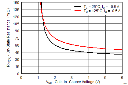 |
Gate Charge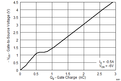 |