-
LM5118 宽电压范围降压/升压控制器
- 1 特性
- 2 应用
- 3 说明
- 4 修订历史记录
- 5 Pin Configuration and Functions
- 6 Specifications
- 7 Detailed Description
-
8 Application and Implementation
- 8.1 Application Information
- 8.2
Typical Application
- 8.2.1 Design Requirements
- 8.2.2
Detailed Design Procedure
- 8.2.2.1 Custom Design With WEBENCH® Tools
- 8.2.2.2 R7 = RT
- 8.2.2.3 Inductor Selection, L1
- 8.2.2.4 R13 = RSENSE
- 8.2.2.5 C15 = CRAMP
- 8.2.2.6 Inductor Current Limit Calculation
- 8.2.2.7 C9 - C12 = Output Capacitors
- 8.2.2.8 D1
- 8.2.2.9 D4
- 8.2.2.10 C1 - C5 = Input Capacitor
- 8.2.2.11 C20
- 8.2.2.12 C8
- 8.2.2.13 C16 = CSS
- 8.2.2.14 R8, R9
- 8.2.2.15 R1, R3, C21
- 8.2.2.16 R2
- 8.2.2.17 Snubber
- 8.2.2.18 Error Amplifier Configuration
- 8.2.3 Application Curves
- 9 Power Supply Recommendations
- 10Layout
- 11器件和文档支持
- 12机械、封装和可订购信息
- 重要声明
DATA SHEET
LM5118 宽电压范围降压/升压控制器
本资源的原文使用英文撰写。 为方便起见,TI 提供了译文;由于翻译过程中可能使用了自动化工具,TI 不保证译文的准确性。 为确认准确性,请务必访问 ti.com 参考最新的英文版本(控制文档)。
1 特性
- 3V 至 75V 的超宽输入电压范围
- 仿真峰值电流模式控制
- 在降压和升压模式之间平滑转换
- 开关频率最高可通过编程设定为 500kHz
- 振荡器同步功能
- 内部高电压偏置稳压器
- 集成了高侧和低侧栅极驱动器
- 可编程软启动时间
- 超低关断电流
- 使能输入宽带宽误差放大器
- 1.5% 反馈基准精度
- 热关断
- 封装:20 引脚 HTSSOP(裸露焊盘)
- 结合使用 LM5118 和 WEBENCH® 电源设计器创建定制设计
2 应用
工业降压/升压电源
3 说明
LM5118 宽电压范围降压/升压开关稳压控制器 具有 使用最少外部组件实现高性能且具成本效益的降压/升压稳压器所需的所有功能。当输入电压低于或高于输出电压时,降压/升压拓扑可使输出电压保持稳定,因此,这款器件非常适合汽车 应用。当输入电压比调节后的输出电压足够大时,LM5118 将作为降压稳压器运行,然后随着输入电压接近输出电压逐渐过渡到相应的降压/升压模式。这种双模式方法可在宽输入电压范围内保持稳压,并且在降压模式下提供最佳的转换效率,同时在模式转换期间提供无干扰的输出。该控制器易于使用,其中包含适用于高侧降压 MOSFET 和低侧升压 MOSFET 的驱动器。此稳压器控制方法基于采用仿真电流斜坡的电流模式控制。仿真电流模式控制可降低脉宽调制电路的噪声敏感度,以便可靠地控制高输入电压 应用中所需的极小占空比。额外保护 功能 包括电流限制、热关断和使能输入。该器件采用功耗增强型 20 引脚 HTSSOP 封装,并且配有利于散热的裸露芯片连接焊盘。
器件信息(1)
| 器件型号 | 封装 | 封装尺寸(标称值) |
|---|---|---|
| LM5118 | HTSSOP (20) | 6.50mm x 4.40mm |
- 如需了解所有可用封装,请参阅数据表末尾的可订购产品附录。
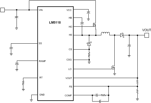
简化电路原理图

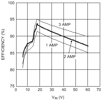
效率与输入电压和输出电流(输出电压 = 12V)

4 修订历史记录
Changes from I Revision (August 2014) to J Revision
- 将汽车器件移到了单独的产品说明书中 (SNVSAX9) Go
- Moved the storage temp parameters to the Absolute Maximum RatingsGo
- Changed junction temperature range from: ±150°C max to: –40°C to 150°CGo
- Changed Handling Ratings table to ESD RatingsGo
- Moved the junction temperature ranges to the condition statementGo
- Removed the VOLL minimum valueGo
- Removed the VOLH minimum valueGo
Changes from H Revision (October 2013) to I Revision
- Changed 产品说明书流程和布局,以符合新的 TI 标准。添加了以下部分:应用和实施;电源建议;布局;器件和文档支持;机械、封装和订购信息Go
- Deleted footnote "These pins must not be raised above VIN."Go
Changes from G Revision (February, 2013) to H Revision
- Deleted VIN Range on Functional Block DiagramGo
- Changed Figure 19Go
- Changed Inductor Selection, L1 TextGo
- Changed Equation 15Go
- Changed Equation 16 Go
- Added Efficiency ParameterGo
- Changed II(PEAK) ValueGo
- Changed I2(PEAK) ValueGo
- Changed R13 = RSENSEText Go
- Added Equation 19 Go
- Added Equation 20 Go
- Changed Equation 21 Go
- Changed Equation 22 Go
- Changed R13(BUCK) ValueGo
- Changed R13(BUCK-BOOST) ValueGo
- Added Inductor Current Limit Calculation SectionGo
- Added Equation 24 Go
- Added Equation 26 Go
- Changed Equation 29 Go
- Changed ESRMAX ValueGo
- Deleted Previous Equation 17Go
- Deleted Previous Equation 18Go
- Changed C1 - C5 = Input Capacitor TextGo
- Changed R8, R9 TextGo
- Changed Equation 38 Go
- Changed R1, R3, C21 TextGo
- Changed Equation 40 Go
- Changed DMIN to DMAXGo
- Changed DMAX ValueGo
- Changed DC Gain(MOD) ValueGo
- Changed ESRZERO ValueGo
- Changed R4, C18, C17 TextGo
- Changed Figure 21Go
- Changed Figure 22Go
- Changed Figure 23Go
- Added Figure 24Go
- Added Figure 25Go
- Added Figure 26Go
Changes from F Revision (February 2013) to G Revision
- Changed layout of National Data Sheet to TI formatGo
5 Pin Configuration and Functions
PWP Package
20-Pin HTSSOP
(Top View)

Pin Descriptions
| PIN | TYPE(1) | DESCRIPTION | |
|---|---|---|---|
| NO. | NAME | ||
| 1 | VIN | P/I | Input supply voltage. |
| 2 | UVLO | I | If the UVLO pin is below 1.23 V, the regulator will be in standby mode (VCC regulator running, switching regulator disabled). When the UVLO pin exceeds 1.23 V, the regulator enters the normal operating mode. An external voltage divider can be used to set an undervoltage shutdown threshold. A fixed 5-µA current is sourced out of the UVLO pin. If a current limit condition exists for 256 consecutive switching cycles, an internal switch pulls the UVLO pin to ground and then releases. |
| 3 | RT | I | The internal oscillator frequency is set with a single resistor between this pin and the AGND pin. The recommended frequency range is 50 kHz to 500 kHz. |
| 4 | EN | I | If the EN pin is below 0.5 V, the regulator will be in a low power state drawing less than 10 µA from VIN. EN must be raised above 3 V for normal operation. |
| 5 | RAMP | I | Ramp control signal. An external capacitor connected between this pin and the AGND pin sets the ramp slope used for emulated current mode control. |
| 6 | AGND | G | Analog ground. |
| 7 | SS | I | Soft Start. An external capacitor and an internal 10-µA current source set the rise time of the error amp reference. The SS pin is held low when VCC is less than the VCC undervoltage threshold (< 3.7 V), when the UVLO pin is low (< 1.23 V), when EN is low (< 0.5 V) or when thermal shutdown is active. |
| 8 | FB | I | Feedback signal from the regulated output. Connect to the inverting input of the internal error amplifier. |
| 9 | COMP | O | Output of the internal error amplifier. The loop compensation network should be connected between COMP and the FB pin. |
| 10 | VOUT | I | Output voltage monitor for emulated current mode control. Connect this pin directly to the regulated output. |
| 11 | SYNC | I | Sync input for switching regulator synchronization to an external clock. |
| 12 | CS | I | Current sense input. Connect to the diode side of the current sense resistor. |
| 13 | CSG | I | Current sense ground input. Connect to the ground side of the current sense resistor. |
| 14 | PGND | G | Power Ground. |
| 15 | LO | O | Boost MOSFET gate drive output. Connect to the gate of the external boost MOSFET. |
| 16 | VCC | P/I/O | Output of the bias regulator. Locally decouple to PGND using a low ESR/ESL capacitor located as close to the controller as possible. |
| 17 | VCCX | P/I | Optional input for an externally supplied bias supply. If the voltage at the VCCX pin is greater than 3.9 V, the internal VCC regulator is disabled and the VCC pin is internally connected to VCCX pin supply. If VCCX is not used, connect to AGND. |
| 18 | HB | I | High-side gate driver supply used in bootstrap operation. The bootstrap capacitor supplies current to charge the high-side MOSFET gate. This capacitor should be placed as close to the controller as possible and connected between HB and HS. |
| 19 | HO | O | Buck MOSFET gate drive output. Connect to the gate of the high-side buck MOSFET through a short, low inductance path. |
| 20 | HS | I | Buck MOSFET source pin. Connect to the source terminal of the high-side buck MOSFET and the bootstrap capacitor. |
| — | EP | — | Solder to the ground plane under the IC to aid in heat dissipation. |
(1) G = Ground, I = Input, O = Output, P = Power