-
ADC32RF42 双通道 14 位 1.5GSPS 模数转换器
- 1 特性
- 2 应用
- 3 说明
- 4 修订历史记录
- 5 Device Family Comparison Table
- 6 Pin Configuration and Functions
- 7 Specifications
- 8 Parameter Measurement Information
-
9 Detailed Description
- 9.1 Overview
- 9.2 Functional Block Diagram
- 9.3
Feature Description
- 9.3.1 Analog Inputs
- 9.3.2 Clock Input
- 9.3.3 SYSREF Input
- 9.3.4 DDC Block
- 9.3.5 NCO Switching
- 9.3.6 SerDes Transmitter Interface
- 9.3.7 Eye Diagrams
- 9.3.8 Alarm Outputs: Power Detectors for AGC Support
- 9.3.9 Power-Down Mode
- 9.3.10 ADC Test Pattern
- 9.4
Device Functional Modes
- 9.4.1 Device Configuration
- 9.4.2
JESD204B Interface
- 9.4.2.1 JESD204B Initial Lane Alignment (ILA)
- 9.4.2.2 JESD204B Frame Assembly
- 9.4.2.3 JESD204B Frame Assembly in Bypass Mode
- 9.4.2.4 JESD204B Frame Assembly with Decimation (Single-Band DDC): Complex Output
- 9.4.2.5 JESD204B Frame Assembly with Decimation (Single-Band DDC): Real Output
- 9.4.2.6 JESD204B Frame Assembly with Decimation (Single-Band DDC): Real Output
- 9.4.2.7 JESD204B Frame Assembly with Decimation (Dual-Band DDC): Complex Output
- 9.4.2.8 JESD204B Frame Assembly with Decimation (Dual-Band DDC): Real Output
- 9.4.3 Serial Interface
- 9.5
Register Maps
- 9.5.1 Example Register Writes
- 9.5.2
Register Descriptions
- 9.5.2.1
General Registers
- 9.5.2.1.1 Register 000h (address = 000h), General Registers
- 9.5.2.1.2 Register 002h (address = 002h), General Registers
- 9.5.2.1.3 Register 003h (address = 003h), General Registers
- 9.5.2.1.4 Register 004h (address = 004h), General Registers
- 9.5.2.1.5 Register 010h (address = 010h), General Registers
- 9.5.2.1.6 Register 011h (address = 011h), General Registers
- 9.5.2.1.7 Register 012h (address = 012h), General Registers
- 9.5.2.1
General Registers
- 9.5.3
Master Page (M = 0)
- 9.5.3.1 Register 020h (address = 020h), Master Page
- 9.5.3.2 Register 032h (address = 032h), Master Page
- 9.5.3.3 Register 039h (address = 039h), Master Page
- 9.5.3.4 Register 03Ch (address = 03Ch), Master Page
- 9.5.3.5 Register 05Ah (address = 05Ah), Master Page
- 9.5.3.6 Register 03Dh (address = 3Dh), Master Page
- 9.5.3.7 Register 057h (address = 057h), Master Page
- 9.5.3.8 Register 058h (address = 058h), Master Page
- 9.5.4 ADC Page (FFh, M = 0)
- 9.5.5 Offset Corr Page Channel A (610000h, M = 1)
- 9.5.6 Offset Corr Page Channel B (610100h, M = 1)
- 9.5.7 Digital Gain Page (610005h, M = 1 for Channel A and 610105h, M = 1 for Channel B)
- 9.5.8 Main Digital Page Channel A (680000h, M = 1)
- 9.5.9 Main Digital Page Channel B (680100h, M = 1)
- 9.5.10
JESD Digital Page (690000h, M = 1)
- 9.5.10.1 Register 001h (address = 001h), JESD Digital Page
- 9.5.10.2 Register 002h (address = 002h ), JESD Digital Page
- 9.5.10.3 Register 003h (address = 003h), JESD Digital Page
- 9.5.10.4 Register 004h (address = 004h), JESD Digital Page
- 9.5.10.5 Register 006h (address = 006h), JESD Digital Page
- 9.5.10.6 Register 007h (address = 007h), JESD Digital Page
- 9.5.10.7 Register 016h (address = 016h), JESD Digital Page
- 9.5.10.8 Register 017h (address = 017h), JESD Digital Page
- 9.5.10.9 Register 032h-035h (address = 032h-035h), JESD Digital Page
- 9.5.10.10 Register 036h (address = 036h), JESD Digital Page
- 9.5.10.11 Register 037h (address = 037h), JESD Digital Page
- 9.5.10.12 Register 03Ch (address = 03Ch), JESD Digital Page
- 9.5.10.13 Register 03Eh (address = 03Eh), JESD Digital Page
- 9.5.11 Special Page Channel A
- 9.5.12 Special Page Channel B
- 9.5.13
Decimation Filter Page
- 9.5.13.1 Register 000h (address = 000h), Decimation Filter Page
- 9.5.13.2 Register 001h (address = 001h), Decimation Filter Page
- 9.5.13.3 Register 002h (address = 2h), Decimation Filter Page
- 9.5.13.4 Register 005h (address = 005h), Decimation Filter Page
- 9.5.13.5 Register 006h (address = 006h), Decimation Filter Page
- 9.5.13.6 Register 007h (address = 007h), Decimation Filter Page
- 9.5.13.7 Register 008h (address = 008h), Decimation Filter Page
- 9.5.13.8 Register 009h (address = 009h), Decimation Filter Page
- 9.5.13.9 Register 00Ah (address = 00Ah), Decimation Filter Page
- 9.5.13.10 Register 00Bh (address = 00Bh), Decimation Filter Page
- 9.5.13.11 Register 00Ch (address = 00Ch), Decimation Filter Page
- 9.5.13.12 Register 00Dh (address = 00Dh), Decimation Filter Page
- 9.5.13.13 Register 00Eh (address = 00Eh), Decimation Filter Page
- 9.5.13.14 Register 00Fh (address = 00Fh), Decimation Filter Page
- 9.5.13.15 Register 010h (address = 010h), Decimation Filter Page
- 9.5.13.16 Register 011h (address = 011h), Decimation Filter Page
- 9.5.13.17 Register 014h (address = 014h), Decimation Filter Page
- 9.5.13.18 Register 016h (address = 016h), Decimation Filter Page
- 9.5.13.19 Register 01Eh (address = 01Eh), Decimation Filter Page
- 9.5.13.20 Register 01Fh (address = 01Fh), Decimation Filter Page
- 9.5.13.21 Register 020h (address = 020h), Decimation Filter Page
- 9.5.13.22 Register 033h-036h (address = 033h-036h), Decimation Filter Page
- 9.5.13.23 Register 037h (address = 037h), Decimation Filter Page
- 9.5.13.24 Register 038h (address = 038h), Decimation Filter Page
- 9.5.13.25 Register 039h (address = 039h), Decimation Filter Page
- 9.5.13.26 Register 03Ah (address = 03Ah), Decimation Filter Page
- 9.5.14
Power Detector Page
- 9.5.14.1 Register 000h (address = 000h), Power Detector Page
- 9.5.14.2 Register 001h-002h (address = 001h-002h), Power Detector Page
- 9.5.14.3 Register 003h (address = 003h), Power Detector Page
- 9.5.14.4 Register 007h-00Ah (address = 007h-00Ah), Power Detector Page
- 9.5.14.5 Register 00Bh-00Ch (address = 00Bh-00Ch), Power Detector Page
- 9.5.14.6 Register 00Dh (address = 00Dh), Power Detector Page
- 9.5.14.7 Register 00Eh (address = 00Eh), Power Detector Page
- 9.5.14.8 Register 00Fh, 010h-012h, and 016h-019h (address = 00Fh, 010h-012h, and 016h-019h), Power Detector Page
- 9.5.14.9 Register 013h-01Ah (address = 013h-01Ah), Power Detector Page
- 9.5.14.10 Register 01Dh-01Eh (address = 01Dh-01Eh), Power Detector Page
- 9.5.14.11 Register 020h (address = 020h), Power Detector Page
- 9.5.14.12 Register 021h (address = 021h), Power Detector Page
- 9.5.14.13 Register 022h-025h (address = 022h-025h), Power Detector Page
- 9.5.14.14 Register 027h (address = 027h), Power Detector Page
- 9.5.14.15 Register 02Bh (address = 02Bh), Power Detector Page
- 9.5.14.16 Register 037h (address = 037h), Power Detector Page
- 9.5.14.17 Register 038h (address = 038h), Power Detector Page
- 9.5.14.18 Power Detector Page (Direct Addressing, 16-Bit Address, 5400h)
- 10Application and Implementation
- 11Power Supply Recommendations
- 12Layout
- 13器件和文档支持
- 14机械、封装和可订购信息
- 重要声明
DATA SHEET
ADC32RF42 双通道 14 位 1.5GSPS 模数转换器
本资源的原文使用英文撰写。 为方便起见,TI 提供了译文;由于翻译过程中可能使用了自动化工具,TI 不保证译文的准确性。 为确认准确性,请务必访问 ti.com 参考最新的英文版本(控制文档)。
1 特性
- 14 位双通道 1.5GSPS ADC
- 本底噪声:–151.8dBFS/Hz
- 射频输入支持的频率最高可达 4GHz
- 孔径抖动:90fs
- 通道隔离:fIN = 1.8GHz 时为 95dB
- 频谱性能(fIN = 950MHz,–2dBFS):
- SNR:61.1dBFS
- SFDR:67dBc(HD2、HD3)
- 频谱性能(fIN = 1.85GHz,–2dBFS):
- 信噪比 (SNR):58.9dBFS
- SFDR:64dBc(HD2、HD3)
- 片上数字下变频器:
- 最多 4 个下变频器 (DDC)(双频带模式)
- 每个 DDC 最多配有 3 个独立数控振荡器 (NCO)
- 提供过压保护的片上输入钳位
- 用于 AGC 支持的带警报引脚的可编程片上功率检测器
- 片上抖动
- 片上输入端接电阻
- 输入满量程:1.35 VPP
- 支持多芯片同步
- JESD204B 接口:
- 基于子类 1 的确定性延迟
- 每通道 4 条信道,高达 12.5Gbps
- 功率耗散:1.5GSPS 时为 2W/通道
- 72 引脚超薄型四方扁平无引线 (VQFN) 封装 (10mm × 10mm)
2 应用
- 多频带、多模式 2G、3G、4G 蜂窝接收器
- 相控阵列雷达
- 电子对抗战
- 线缆基础设施
- 无线宽带
- 高速数字转换器
- 软件定义无线电
- 通信测试设备
- 微波和毫米波接收器
3 说明
ADC32RF42 器件是一款 14 位 1.5GSPS 双通道模数转换器 (ADC),支持输入频率高达 4GHz 及以上的射频采样。ADC32RF42 专为高信噪比 (SNR) 设计,其噪声频谱密度为 –151.8dBFS/Hz,并可在较大输入频率范围提供动态范围和通道隔离。经缓冲的模拟输入配有片上端接电阻,可在较宽频率范围内提供统一输入阻抗并最大程度地降低采样和保持毛刺脉冲能量。
每个 ADC 通道均可连接到一个双频带数字下变频器 (DDC),每个 DDC 最多连接三个独立的 16 位数控振荡器 (NCO) 用于相位相干跳频。此外,ADC 还配有前端峰值和 RMS 功率检测器及报警功能,用以支持外部自动增益控制 (AGC) 算法。
ADC32RF42 支持具有基于子类 1 确定性延迟的 JESD204B 串行接口,其数据速率高达 12.5Gbps,每个 ADC 最多具有四条信道。该器件采用 72 引脚 VQFN 封装 (10mm × 10mm),支持工业级温度范围(-40℃ 至 +85°C)。
器件信息(1)
| 器件型号 | 封装 | 封装尺寸(标称值) |
|---|---|---|
| ADC32RF42 | VQFN (72) | 10.00mm x 10.00mm |
- 要了解所有可用封装,请参见数据表末尾的可订购产品附录。
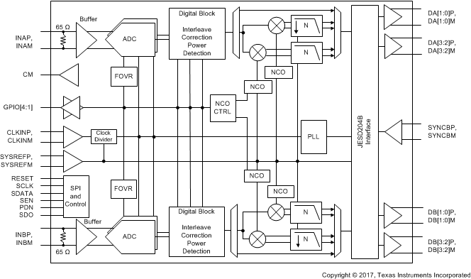
简化框图
4 修订历史记录
| 日期 | 修订版本 | 注释 |
|---|---|---|
| 2017 年 5 月 | * | 首次发布。 |
5 Device Family Comparison Table
| PART NUMBER | SPEED GRADE (MSPS) | RESOLUTION (Bits) | CHANNELS |
|---|---|---|---|
| ADC32RF45 | 3000 | 14 | 2 |
| ADC32RF44 | 2600 | 14 | 2 |
| ADC32RF42 | 1500 | 14 | 2 |
6 Pin Configuration and Functions
RMP Package
72-Pin VQFN
Top View
Pin Functions
| NAME | NO. | I/O | DESCRIPTION |
|---|---|---|---|
| INPUT, REFERENCE | |||
| INAM | 41 | I | Differential analog input for channel A |
| INAP | 42 | ||
| INBM | 14 | I | Differential analog input for channel B |
| INBP | 13 | ||
| CM | 22 | O | Common-mode voltage for analog inputs, 1.2 V |
| CLOCK, SYNC | |||
| CLKINM | 28 | I | Differential clock input for the analog-to-digital converter (ADC). This pin has an internal differential 100-Ω termination. |
| CLKINP | 27 | ||
| SYSREFM | 34 | I | External sync input. This pin has an internal, differential 100-Ω termination and requires external biasing. |
| SYSREFP | 33 | ||
| GPIO1 | 19 | I/O | GPIO control pin; configured through the SPI. This pin can be configured to be either a fast overrange output for channel A and B, a fast detect alarm signal from the peak power detect, or a numerically-controlled oscillator (NCO) control. GPIO 4 (pin 63) can also be configured as a single-ended SYNCB input. |
| GPIO2 | 20 | ||
| GPIO3 | 21 | ||
| GPIO4 | 63 | ||
| CONTROL, SERIAL | |||
| RESET | 48 | I | Hardware reset; active high. This pin has an internal 20-kΩ pulldown resistor. |
| SCLK | 6 | I | Serial interface clock input. This pin has an internal 20-kΩ pulldown resistor. |
| SDIN | 5 | I/O | Serial interface data input. This pin has an internal 20-kΩ pulldown resistor. SDIN can be data input in 4-wire mode, data input and output in 3-wire mode. |
| SEN | 7 | I | Serial interface enable. This pin has an internal 20-kΩ pullup resistor to DVDD. |
| SDOUT | 11 | O | Serial interface data output in 4-wire mode |
| PDN | 50 | I | Power down; active high. This pin can be configured through an SPI register setting and can be configured to a fast overrange output channel B through the SPI. This pin has an internal 20-kΩ pulldown resistor. |
| DATA INTERFACE | |||
| DA0M | 62 | O | JESD204B serial data output for channel A |
| DA0P | 61 | ||
| DA1M | 59 | ||
| DA1P | 58 | ||
| DA2M | 56 | ||
| DA2P | 55 | ||
| DA3M | 54 | ||
| DA3P | 53 | ||
| DB0M | 65 | O | JESD204B serial data output for channel B |
| DB0P | 66 | ||
| DB1M | 68 | ||
| DB1P | 69 | ||
| DB2M | 71 | ||
| DB2P | 72 | ||
| DB3M | 1 | ||
| DB3P | 2 | ||
| SYNCBM | 36 | I | Synchronization input for the JESD204B port. This pin has an LVDS or 1.8-V logic input, an optional on-chip 100-Ω termination, and is selectable through the SPI. This pin requires external biasing. |
| SYNCBP | 35 | ||
| POWER SUPPLY | |||
| AVDD19 | 10, 16, 24, 31, 39, 45 | I | Analog 1.9-V power supply |
| AVDD | 9, 12, 15, 17, 25, 30, 38, 40, 43, 44, 46 | I | Analog 1.15-V power supply |
| DVDD | 4, 8, 47, 51, 57, 64, 70 | I | Digital 1.15 V-power supply, including the JESD204B transmitter |
| GND | 3, 18, 23, 26, 29, 32, 37, 49, 52, 60, 67 | I | Ground; shorted to thermal pad inside device |
7 Specifications
7.1 Absolute Maximum Ratings
over operating free-air temperature range (unless otherwise noted)(1)| MIN | MAX | UNIT | ||
|---|---|---|---|---|
| Supply voltage range | AVDD19 | –0.3 | 2.1 | V |
| AVDD | –0.3 | 1.4 | ||
| DVDD | –0.3 | 1.4 | ||
| Voltage applied to input pins | INAP, INAM and INBP, INBM | –0.3 | AVDD19 + 0.3 | V |
| CLKINP, CLKINM | –0.3 | AVDD + 0.6 | ||
| SYSREFP, SYSREFM, SYNCBP, SYNCBM | –0.3 | AVDD + 0.6 | ||
| SCLK, SEN, SDIN, RESET, PDN, GPIO1, GPIO2, GPIO3, GPIO4 | –0.2 | AVDD19 + 0.2 | ||
| Voltage applied to output pins | –0.3 | 2.2 | V | |
| Temperature | Operating free-air, TA | –40 | 85 | °C |
| Storage, Tstg | –65 | 150 | ||
(1) Stresses beyond those listed under Absolute Maximum Ratings may cause permanent damage to the device. These are stress ratings only, which do not imply functional operation of the device at these or any other conditions beyond those indicated under Recommended Operating Conditions. Exposure to absolute-maximum-rated conditions for extended periods may affect device reliability.
7.2 ESD Ratings
| VALUE | UNIT | |||
|---|---|---|---|---|
| V(ESD) | Electrostatic discharge | Human-body model (HBM), per ANSI/ESDA/JEDEC JS-001(1) | ±1000 | V |
| Charged-device model (CDM), per JEDEC specification JESD22-C101(2) | ±500 | |||
(1) JEDEC document JEP155 states that 500-V HBM allows safe manufacturing with a standard ESD control process.
(2) JEDEC document JEP157 states that 250-V CDM allows safe manufacturing with a standard ESD control process.
7.3 Recommended Operating Conditions
over operating free-air temperature range (unless otherwise noted)| MIN | NOM | MAX | UNIT | ||
|---|---|---|---|---|---|
| Supply voltage(2) | AVDD19 | 1.8 | 1.9 | 2.0 | V |
| AVDD | 1.1 | 1.15 | 1.25 | ||
| DVDD | 1.1 | 1.15 | 1.2 | ||
| Temperature | Operating free-air, TA | –40 | 85 | °C | |
| Operating junction, TJ | 105(1) | 125 |
(1) Prolonged use above this junction temperature may increase the device failure-in-time (FIT) rate.
(2) Always power up the DVDD supply (1.15 V) before the AVDD19 (1.9 V) supply. The AVDD (1.15 V) supply can come up in any order.
7.4 Thermal Information
| THERMAL METRIC(1) | ADC32RF42 | UNIT | |
|---|---|---|---|
| RMP (VQFN) | |||
| 72 PINS | |||
| RθJA | Junction-to-ambient thermal resistance | 21.8 | °C/W |
| RθJC(top) | Junction-to-case (top) thermal resistance | 4.4 | °C/W |
| RθJB | Junction-to-board thermal resistance | 2.0 | °C/W |
| ψJT | Junction-to-top characterization parameter | 0.1 | °C/W |
| ψJB | Junction-to-board characterization parameter | 2.0 | °C/W |
| RθJC(bot) | Junction-to-case (bottom) thermal resistance | 0.2 | °C/W |
(1) For more information about traditional and new thermal metrics, see the Semiconductor and IC Package Thermal Metrics application report.
7.5 Electrical Characteristics
typical values are specified at an ambient temperature of 25°C; minimum and maximum values are specified over an ambient temperature range of –40°C to +85°C; and ADC sampling rate = 1.5 GHz, 50% clock duty cycle, AVDD19 = 1.9 V, AVDD = 1.15 V, DVDD = 1.15 V, –2-dBFS differential input, and 0-dB digital gain (unless otherwise noted)| PARAMETER | TEST CONDITIONS | MIN | TYP | MAX | UNIT | |
|---|---|---|---|---|---|---|
| POWER CONSUMPTION(4) (Dual-Channel Operation, Both Channels A and B are Active; DDC Bypass Mode(3)) | ||||||
| IAVDD19 | 1.9-V analog supply current | 14-bit, bypass mode, fS = 1.5 GSPS | 1150 | 1969 | mA | |
| IAVDD | 1.15-V analog supply current | 14-bit, bypass mode, fS = 1.5 GSPS | 604 | 1079 | mA | |
| IDVDD | 1.15-V digital supply current | 14-bit, bypass mode, fS = 1.5 GSPS | 1000 | 1846 | mA | |
| PD | Power dissipation | 14-bit, bypass mode, fS = 1.5 GSPS | 4.03 | 6.95 | W | |
| Global power-down power dissipation | 360 | mW | ||||
| ANALOG INPUTS | ||||||
| Resolution | 14 | Bits | ||||
| Differential input full-scale | 1.35 | VPP | ||||
| VIC | Input common-mode voltage | 1.2(5) | V | |||
| RIN | Input resistance | Differential resistance at dc | 65 | Ω | ||
| CIN | Input capacitance | Differential capacitance at dc | 2 | pF | ||
| VCM common-mode voltage output | 1.2 | V | ||||
| Analog input bandwidth (–3-dB point) |
ADC driven with 50-Ω source | 3200 | MHz | |||
| ISOLATION | ||||||
| Crosstalk isolation between channel A and channel B(1) | fIN = 100 MHz | 100 | dBc | |||
| fIN = 900 MHz | 99 | |||||
| fIN = 1800 MHz | 95 | |||||
| fIN = 2700 MHz | 86 | |||||
| fIN = 3500 MHz | 85 | |||||
| CLOCK INPUT(2) | ||||||
| Input clock frequency | 750 | 1500 | MHz | |||
| Differential (peak-to-peak) input clock amplitude | 0.5 | 1.5 | 2.5 | VPP | ||
| Input clock duty cycle | 45% | 50% | 55% | |||
| Internal clock biasing | 1.0 | V | ||||
| Internal clock termination (differential) | 100 | Ω | ||||
(1) Crosstalk is measured with a –2-dBFS input signal on aggressor channel and no input on the victim channel.
(2) See Figure 32.
(3) Full-scale signal is applied to the analog inputs of all active channels.
(4) See the Power Consumption in Different Modes section for more details.
(5) When used in dc-coupling mode, the common-mode voltage at the analog inputs should be kept within VCM ±25 mV for best performance.
7.6 AC Performance Characteristics
typical values specified at an ambient temperature of 25°C; minimum and maximum values are specified over an ambient temperature range of –40°C to +85°C; and ADC sampling rate = 1.5 GHz, 50% clock duty cycle, AVDD19 = 1.9 V, AVDD = 1.15 V, DVDD = 1.15 V, –2-dBFS differential input, and 0-dB digital gain (unless otherwise noted)| PARAMETER | TEST CONDITIONS | MIN(2) | NOM | MAX | UNIT | ||
|---|---|---|---|---|---|---|---|
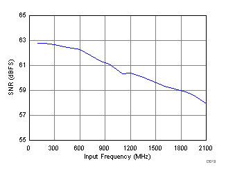
| SNR | Signal-to-noise ratio | fIN = 100 MHz, AOUT = –2 dBFS | 62.8 | dBFS | |||
| fIN = 300 MHz, AOUT = –2 dBFS | 62.6 | ||||||
| fIN = 950 MHz, AOUT = –2 dBFS | 61.1 | ||||||
| fIN = 1200 MHz, AOUT = –2 dBFS | 60.4 | ||||||
| fIN = 1350 MHz, AOUT = –2 dBFS | 60.0 | ||||||
| fIN = 1850 MHz, AOUT = –2 dBFS | 58.9 | ||||||
| fIN = 2100 MHz, AOUT = –2 dBFS | 57.9 | ||||||
| NSD | Noise spectral density averaged across the Nyquist zone | fIN = 100 MHz, AOUT = –2 dBFS | 151.6 | dBFS/Hz | |||
| fIN = 300 MHz, AOUT = –2 dBFS | 151.4 | ||||||
| fIN = 950 MHz, AOUT = –2 dBFS | 149.8 | ||||||
| fIN = 1200 MHz, AOUT = –2 dBFS | 149.1 | ||||||
| fIN = 1350 MHz, AOUT = –2 dBFS | 148.8 | ||||||
| fIN = 1850 MHz, AOUT = –2 dBFS | 147.6 | ||||||
| fIN = 2100 MHz, AOUT = –2 dBFS | 146.7 | ||||||
| Small-signal SNR | fIN = 950 MHz, AOUT = –40 dBFS | 63.0 | dBFS | ||||
| NF(1) | Input noise figure | fIN = 950 MHz, AOUT = –40 dBFS | 27.7 | dB | |||
| SINAD | Signal-to-noise and distortion ratio | fIN = 100 MHz, AOUT = –2 dBFS | 61.4 | dBFS | |||
| fIN = 300 MHz, AOUT = –2 dBFS | 61.0 | ||||||
| fIN = 950 MHz, AOUT = –2 dBFS | 60.9 | ||||||
| fIN = 1200 MHz, AOUT = –2 dBFS | 59.9 | ||||||
| fIN = 1350 MHz, AOUT = –2 dBFS | 59.2 | ||||||
| fIN = 1850 MHz, AOUT = –2 dBFS | 58.2 | ||||||
| fIN = 2100 MHz, AOUT = –2 dBFS | 55.8 | ||||||
| ENOB | Effective number of bits | fIN = 100 MHz, AOUT = –2 dBFS | 9.9 | Bits | |||
| fIN = 300 MHz, AOUT = –2 dBFS | 9.8 | ||||||
| fIN = 950 MHz, AOUT = –2 dBFS | 9.8 | ||||||
| fIN = 1200 MHz, AOUT = –2 dBFS | 9.6 | ||||||
| fIN = 1350 MHz, AOUT = –2 dBFS | 9.5 | ||||||
| fIN = 1850 MHz, AOUT = –2 dBFS | 9.4 | ||||||
| fIN = 2100 MHz, AOUT = –2 dBFS | 9.0 | ||||||
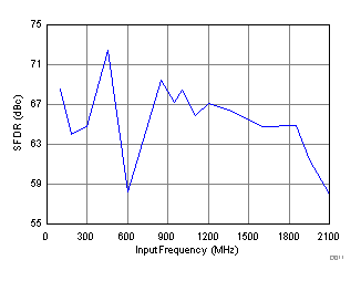
| SFDR | Spurious-free dynamic range | fIN = 100 MHz, AOUT = –2 dBFS | 67 | dBc | |||
| fIN = 300 MHz, AOUT = –2 dBFS | 64 | ||||||
| fIN = 950 MHz, AOUT = –2 dBFS | 70 | ||||||
| fIN = 1200 MHz, AOUT = –2 dBFS | 67 | ||||||
| fIN = 1350 MHz, AOUT = –2 dBFS | 66 | ||||||
| fIN = 1850 MHz, AOUT = –2 dBFS | 64 | ||||||
| fIN = 2100 MHz, AOUT = –2 dBFS | 58 | ||||||
| HD2 | Second-order harmonic distortion | fIN = 100 MHz, AOUT = –2 dBFS | 68 | dBc | |||
| fIN = 300 MHz, AOUT = –2 dBFS | 64 | ||||||
| fIN = 950 MHz, AOUT = –2 dBFS | 72 | ||||||
| fIN = 1200 MHz, AOUT = –2 dBFS | 70 | ||||||
| fIN = 1350 MHz, AOUT = –2 dBFS | 67 | ||||||
| fIN = 1850 MHz, AOUT = –2 dBFS | 64 | ||||||
| fIN = 2100 MHz, AOUT = –2 dBFS | 58 | ||||||
| HD3 | Third-order harmonic distortion | fIN = 100 MHz, AOUT = –2 dBFS | 67 | dBc | |||
| fIN = 300 MHz, AOUT = –2 dBFS | 71 | ||||||
| fIN = 950 MHz, AOUT = –2 dBFS | 70 | ||||||
| fIN = 1200 MHz, AOUT = –2 dBFS | 67 | ||||||
| fIN = 1350 MHz, AOUT = –2 dBFS | 70 | ||||||
| fIN = 1850 MHz, AOUT = –2 dBFS | 73 | ||||||
| fIN = 2100 MHz, AOUT = –2 dBFS | 66 | ||||||
| HD4, HD5 | Fourth- and fifth-order harmonic distortion | fIN = 100 MHz, AOUT = –2 dBFS | 89 | dBc | |||
| fIN = 300 MHz, AOUT = –2 dBFS | 84 | ||||||
| fIN = 950 MHz, AOUT = –2 dBFS | 85 | ||||||
| fIN = 1200 MHz, AOUT = –2 dBFS | 83 | ||||||
| fIN = 1350 MHz, AOUT = –2 dBFS | 85 | ||||||
| fIN = 1850 MHz, AOUT = –2 dBFS | 83 | ||||||
| fIN = 2100 MHz, AOUT = –2 dBFS | 82 | ||||||
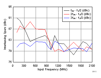
| IL spur | Interleaving spur: fS / 2 – fIN, |
fIN = 100 MHz, AOUT = –2 dBFS | 91 | dBc | |||
| fIN = 300 MHz, AOUT = –2 dBFS | 87 | ||||||
| fIN = 950 MHz, AOUT = –2 dBFS | 83 | ||||||
| fIN = 1200 MHz, AOUT = –2 dBFS | 82 | ||||||
| fIN = 1350 MHz, AOUT = –2 dBFS | 82 | ||||||
| fIN = 1850 MHz, AOUT = –2 dBFS | 82 | ||||||
| fIN = 2100 MHz, AOUT = –2 dBFS | 80 | ||||||
| HD2 IL | Interleaving spur for HD2: fS / 2 – HD2 |
fIN = 100 MHz, AOUT = –2 dBFS | 86 | dBc | |||
| fIN = 300 MHz, AOUT = –2 dBFS | 87 | ||||||
| fIN = 950 MHz, AOUT = –2 dBFS | 83 | ||||||
| fIN = 1200 MHz, AOUT = –2 dBFS | 80 | ||||||
| fIN = 1350 MHz, AOUT = –2 dBFS | 79 | ||||||
| fIN = 1850 MHz, AOUT = –2 dBFS | 79 | ||||||
| fIN = 2100 MHz, AOUT = –2 dBFS | 80 | ||||||
| Worst spur | Spurious-free dynamic range (excluding HD2, HD3, HD4, HD5, and interleaving spurs IL and HD2 IL) | fIN = 100 MHz, AOUT = –2 dBFS | 80 | dBc | |||
| fIN = 300 MHz, AOUT = –2 dBFS | 82 | ||||||
| fIN = 950 MHz, AOUT = –2 dBFS | 80 | ||||||
| fIN = 1200 MHz, AOUT = –2 dBFS | 82 | ||||||
| fIN = 1350 MHz, AOUT = –2 dBFS | 79 | ||||||
| fIN = 1850 MHz, AOUT = –2 dBFS | 80 | ||||||
| fIN = 2100 MHz, AOUT = –2 dBFS | 81 | ||||||
| IMD3 | Third-order intermodulation distortion | fIN1 = 940 MHz, fIN2 = 960 MHz, AOUT = –8 dBFS (each tone) |
75 | dBFS | |||
(1) The ADC internal resistance = 65 Ω, the driving source resistance = 50 Ω.
(2) Minimum values are specified at AOUT = –3 dBFS.
7.7 Digital Requirements
typical values are specified at an ambient temperature of 25°C; minimum and maximum values are specified over an ambient temperature range of –40°C to +85°C; and ADC sampling rate = 1.5 GHz, 50% clock duty cycle, AVDD19 = 1.9 V, AVDD = 1.15 V, DVDD = 1.15 V, –2-dBFS differential input, and 0-dB digital gain (unless otherwise noted)| PARAMETER | TEST CONDITIONS | MIN | NOM | MAX | UNIT | |
|---|---|---|---|---|---|---|
| DIGITAL INPUTS (RESET, SCLK, SEN, SDIN, PDN, GPIO1, GPIO2, GPIO3, GPIO4) | ||||||
| VIH | High-level input voltage | 0.8 | V | |||
| VIL | Low-level input voltage | 0.4 | V | |||
| IIH | High-level input current | 50 | µA | |||
| IIL | Low-level input current | –50 | µA | |||
| Ci | Input capacitance | 4 | pF | |||
| DIGITAL OUTPUTS (SDOUT, GPIO1, GPIO2, GPIO3, GPIO4) | ||||||
| VOH | High-level output voltage | AVDD19–0.1 | AVDD19 | V | ||
| VOL | Low-level output voltage | 0.1 | V | |||
| DIGITAL INPUTS (SYSREFP and SYSREFM; SYNCBP and SYNCBM; Requires External Biasing) | ||||||
| VID | Differential input voltage | 350 | 450 | 800 | mVPP | |
| VCM | Input common-mode voltage | 1.05 | 1.2 | 1.325 | V | |
| DIGITAL OUTPUTS (JESD204B Interface: DA[3:0], DB[3:0], Meets JESD204B LV-0IF-11G-SR Standard) | ||||||
| |VOD| | Output differential voltage | 700 | mVPP | |||
| |VOCM| | Output common-mode voltage | 450 | mV | |||
| Transmitter short-circuit current | Transmitter pins shorted to any voltage between –0.25 V and 1.45 V | –100 | 100 | mA | ||
| zos | Single-ended output impedance | 50 | Ω | |||
| Co | Output capacitance | Output capacitance inside the device, from either output to ground |
2 | pF | ||
7.8 Timing Requirements
typical values are specified at an ambient temperature of 25°C; minimum and maximum values are specified over an ambient temperature range of –40°C to +85°C; and ADC sampling rate = 2.6 GHz, 50% clock duty cycle, AVDD19 = 1.9 V, AVDD = 1.15 V, DVDD = 1.15 V, –2-dBFS differential input, and 0-dB digital gain (unless otherwise noted)| MIN | NOM | MAX | UNIT | |||
|---|---|---|---|---|---|---|
| SAMPLE TIMING | ||||||
| Aperture delay | 250 | 750 | ps | |||
| Aperture delay matching between two channels on the same device | ±15 | ps | ||||
| Aperture delay matching between two devices at the same temperature and supply voltage |
±150 | ps | ||||
| Aperture jitter, clock amplitude = 2 VPP | 90 | fS | ||||
| Fast overrange latency, ADC sample to FOVR indication on GPIO pins | 70 | Input clock cycles | ||||
| tPD | Propagation delay time: logic gates and output buffer delay (does not change with fS) |
6 | ns | |||
| SYSREF TIMING(1) | ||||||
| tSU_SYSREF | SYSREF setup time: referenced to clock rising edge, 1.5 GSPS | 140 | 70 | ps | ||
| tH_SYSREF | SYSREF hold time: referenced to clock rising edge, 1.5 GSPS | 50 | 20 | ps | ||
| Valid transition window sampling period: tSU_SYSREF – tH_SYSREF, 1.5 GSPS | 476 | ps | ||||
| JESD OUTPUT INTERFACE TIMING | ||||||
| UI | Unit interval: 12.5 Gbps | 80 | 100 | 400 | ps | |
| Serial output data rate | 2.5 | 10.0 | 12.5 | Gbps | ||
| Rise, fall times: 1-pF, single-ended load capacitance to ground | 60 | ps | ||||
| Total jitter: BER of 1E-15 and lane rate = 12.5 Gbps | 25 | %UI | ||||
| Random jitter: BER of 1E-15 and lane rate = 12.5 Gbps | 0.99 | %UI, rms | ||||
| Deterministic jitter: BER of 1E-15 and lane rate = 12.5 Gbps | 9.1 | %UI, pk-pk |
||||
(1) Common-mode voltage for the SYSREF input is kept at 1.2 V.
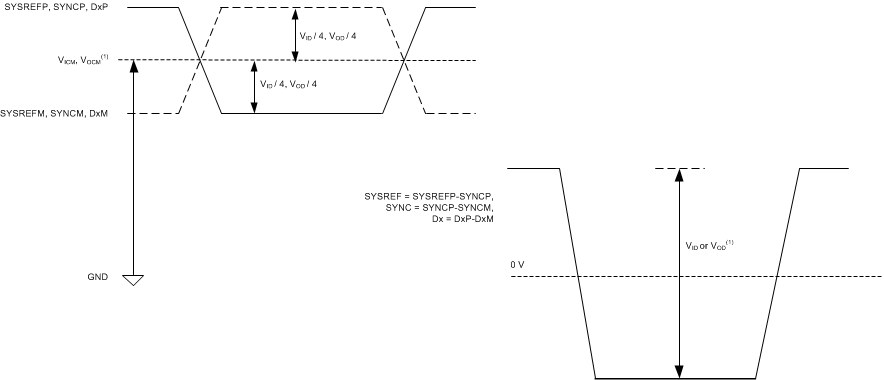
VOCM is not the same as VICM. Similarly, VOD is not the same as VID.
Figure 1. Logic Levels for Digital Inputs and Outputs
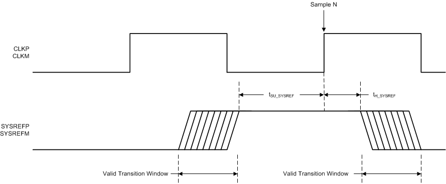 Figure 2. SYSREF Timing Diagram
7.9 Typical Characteristics
typical values are specified at an ambient temperature of 25°C; minimum and maximum values are specified over an ambient temperature range of –40°C to +85°C; and ADC sampling rate = 1.5 GHz, 65536 points FFT, 50% clock duty cycle, AVDD19 = 1.9 V, AVDD = 1.15 V, DVDD = 1.15 V, –2-dBFS differential input, and 0-dB digital gain (unless otherwise noted)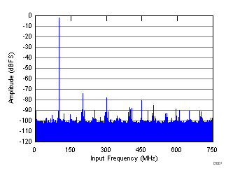
| SFDR = 73 dBc, SNR = 62.4 dBFS, SINAD = 62 dBFS, THD = 71 dBc, HD2 = –75 dBFS, HD3 = –78 dBFS, SFDR (non HD2, HD3) = 85 dBc, IL spur = 81 dBFS |
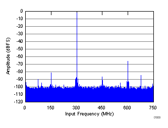
| SFDR = 65 dBc, SNR = 62.3 dBFS, SINAD = 61 dBFS, THD = 64 dBc, HD2 = –67 dBFS, HD3 = –75 dBFS, SFDR (non HD2, HD3) = 74 dBc, IL spur = 82 dBFS |
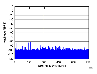
| SFDR = 72 dBc, SNR = 60.2 dBFS, SINAD = 60 dBFS, THD = 71 dBc, HD2 = –74 dBFS, HD3 = –87 dBFS, SFDR (non HD2, HD3) = 80 dBFS, IL spur = 80 dBFS |
||
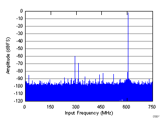
| SFDR = 59 dBc, SNR = 57.9 dBFS, SINAD = 56 dBFS, HD2 = –61 dBFS, HD3 = –69 dBFS, SFDR (non HD2, HD3) = 81 dBc, THD = 58 dBc, IL spur = 83 dBFS |
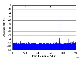
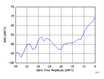
| fIN1 = 940 MHz, fIN2 = 960 MHz, AOUT = –36 dBFS, IMD = 94 dBFS |
| fIN = 950 MHz, AIN = –2 dBFS |
| fIN = 950 MHz, AIN = –2 dBFS |
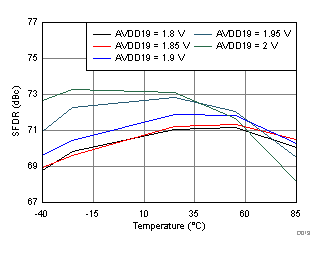
| fIN = 950 MHz, AIN = –2 dBFS |
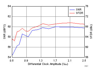
| fIN = 950 MHz, AIN = –2 dBFS |
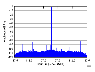
| fIN = 1850 MHz, AIN = –2 dBFS, SNR = 63.8 dBFS, SFDR (includes IL) = 78 dBc, fS = 1500 MSPS |
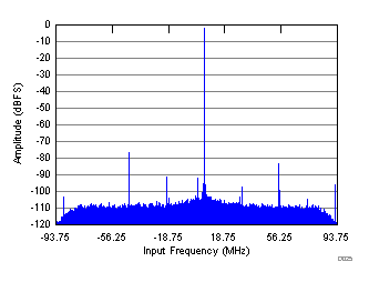
| fIN = 1850 MHz, AIN = –2 dBFS, SNR = 66 dBFS, SFDR (includes IL) = 77 dBc, fS = 1500 MSPS |

| fIN = 1850 MHz, AIN = –2 dBFS, SNR = 65.9 dBFS, SFDR (includes IL) = 74 dBc, fS = 1500 MSPS |
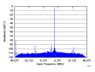
| fIN = 1850 MHz, AIN = –2 dBFS, SNR = 68.1 dBFS, SFDR (includes IL) = 80.9 dBc, fS = 1500 MSPS |
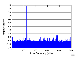
| SFDR = 65 dBc, SNR = 62.3 dBFS, SINAD = 61 dBFS, THD = 64 dBc, HD2 = –67 dBFS, HD3 = –73 dBFS, SFDR (non HD2, HD3) = 89 dBc, IL spur = 81 dBFS |
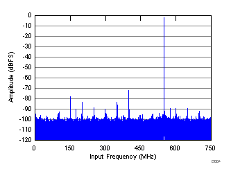
| SFDR = 70 dBc, SNR = 60.8 dBFS, SINAD = 60 dBFS, THD = 69 dBc, HD2 = –72 dBFS, HD3 = –78 dBFS, SFDR (non HD2, HD3) = 81 dBc, IL spur = 82 dBFS |
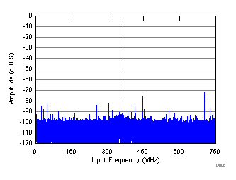
| SFDR = 70 dBc, SNR = 58.7 dBFS, SINAD = 58 dBFS, HD2 = –72 dBFS, HD3 = –75 dBFS, SFDR (non HD2, HD3) = 79 dBc, THD = 68 dBc, IL spur = 80 dBFS |
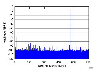
| fIN1 = 940 MHz, fIN2 = 960 MHz, AOUT = –8 dBFS, IMD = 75 dBFS |
||
| fIN = 950 MHz, AIN = –2 dBFS |
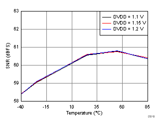
| fIN = 950 MHz, AIN = –2 dBFS |
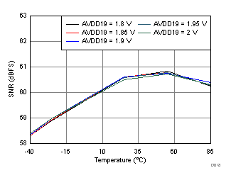
| fIN = 950 MHz, AIN = –2 dBFS |
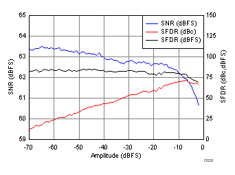
| fIN = 950 MHz, AIN = –2 dBFS |
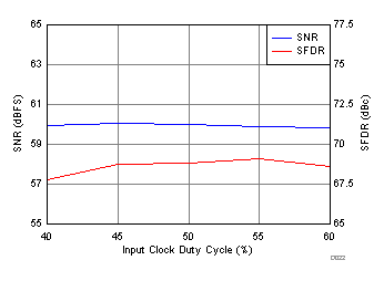
| fIN = 950 MHz, AIN = –2 dBFS |
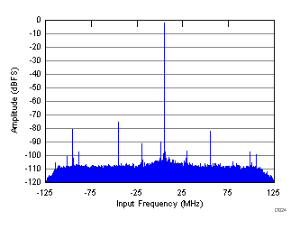
| fIN = 1850 MHz, AIN = –2 dBFS, SNR = 65 dBFS, SFDR (includes IL) = 75 dBc, fS = 1500 MSPS |
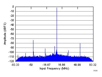
| fIN = 1850 MHz, AIN = –2 dBFS, SNR = 65.8 dBFS, SFDR (includes IL) = 74 dBc, fS = 1500 MSPS |
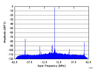
| fIN = 1850 MHz, AIN = –2 dBFS, SNR = 66.4 dBFS, SFDR (includes IL) = 74.1 dBc, fS = 1500 MSPS |