-
TPS53313 集成开关的高效 6A 降压稳压器
- 1 特性
- 2 应用
- 3 说明
- 4 修订历史记录
- 5 Pin Configuration and Functions
- 6 Specifications
- 7 Detailed Description
- 8 Application and Implementation
- 9 Power Supply Recommendations
- 10Layout
- 11器件和文档支持
- 12机械、封装和可订购信息
- 重要声明
TPS53313 集成开关的高效 6A 降压稳压器
1 特性
- 4.5V 至 16V 转换电压范围
- 可调节输出电压范围:0.6V 至 0.7 × VIN
- 6A 持续输出电流
- 支持所有多层陶瓷电容 (MLCC) 输出电容
- 可选跳跃模式或强制连续导通模式 (CCM)
- 可选软启动时间(1ms、3ms 或 6ms)
- 可选 4A-5A、6A 或 9A 峰值电流限值
- 优化了轻负载与重负载条件下的效率
- 电压模式控制
- 可编程开关频率范围:250kHz 至 1.5MHz
- 同步至外部时钟
- 针对过零检测和过流保护提供 RDS(on) 感测
- 软停止输出在禁用期间放电
- 在断续模式下提供过流、过压和欠压保护
- 过热保护
- 开漏电源正常指示
- 内部自举开关
- 4mm × 4mm 24 引脚超薄四方扁平无引线 (VQFN) 封装
2 应用
- 电压为 5V 的 负载点 (POL) 应用
- 12V 降压电压轨
3 说明
TPS53313 提供集成两个 N 沟道金属氧化物半导体场效应晶体管 (MOSFET) 的 5V 或 12V 同步降压转换器。由于低RDS(接通)和TI私有的 SmoothPWM™跳跃模式操作可优化轻载条件下的效率,同时不影响输出电压纹波。
TPS53313 具有 可编程开关频率(250kHz 至 1.5MHz),可选择跳跃模式或强制 CCM 模式操作。该器件提供预偏置启动、软停止、集成自举开关、电源正常功能和 EN/输入电压锁定 (UVLO) 保护。该器件支持 4.5V 至 16V 范围内的输入电压,无需额外使用偏置电压。可调节输出电压范围:0.6V 至 0.7 × VIN。
TPS53313 采用 4mm × 4mm 24 VQFN 封装(绿色环保,符合 RoHS 标准并且无铅),额定运行温度范围为 -40°C 至 85°C。
器件信息(1)
| 器件型号 | 封装 | 封装尺寸(标称值) |
|---|---|---|
| TPS53313 | VQFN (24) | 4.00mm x 4.00mm |
- 要了解所有可用封装,请见数据表末尾的可订购产品附录。
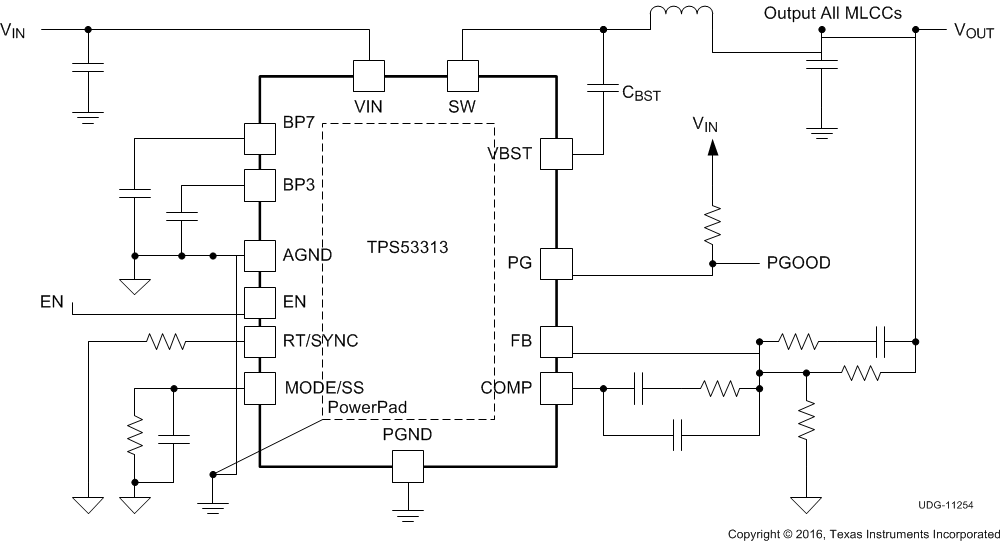
典型应用电路
5 Pin Configuration and Functions
Pin Functions
| PIN | TYPE(1) | DESCRIPTION | |
|---|---|---|---|
| NO. | NAME | ||
| 1 | EN | I | Enable pin |
| 2 | PG | O | Power good output flag. Open drain output. Pull up to an external rail through a resistor. |
| 3 | VIN | P | Gate driver supply and power conversion voltage |
| 4 | VIN | P | Gate driver supply and power conversion voltage |
| 5 | VIN | P | Gate driver supply and power conversion voltage |
| 6 | VIN | P | Gate driver supply and power conversion voltage |
| 7 | PGND | P | Device power ground terminal |
| 8 | PGND | P | Device power ground terminal |
| 9 | PGND | P | Device power ground terminal |
| 10 | PGND | P | Device power ground terminal |
| 11 | PGND | P | Device power ground terminal |
| 12 | PGND | P | Device power ground terminal |
| 13 | SW | O | Output inductor connection to integrated power devices |
| 14 | SW | O | Output inductor connection to integrated power devices |
| 15 | SW | O | Output inductor connection to integrated power devices |
| 16 | SW | O | Output inductor connection to integrated power devices |
| 17 | VBST | P | Supply input for high-side MOSFET (bootstrap terminal). Connect capacitor from this pin to SW terminal. |
| 18 | BP7 | P | Bias for internal circuitry and driver |
| 19 | BP3 | P | Input bias supply for analog functions |
| 20 | AGND | G | Device analog ground terminal |
| 21 | RT/SYNC | I/O | Synchronized to external clock. Program the switching frequency by connecting with a resistor to GND. |
| 22 | MODE/SS | I | Mode configuration pin. Connect with a resistor to GND sets different modes and soft-start time, parallel a capacitor (or no capacitor) with the resistor changes the current limit threshold. Shorting MODE/SS pin to supply inhibits the device; shorting MODE/SS pin to AGND is equivalent to 10-kΩ resistor setting is not recommended (see Table 1 and Table 2 for resistor and capacitor settings). |
| 23 | COMP | O | Error amplifier compensation terminal. Type III compensation method is generally recommended for stability. |
| 24 | FB | I | Voltage feedback pin. Use for OVP, UVP, and power good determination |
6 Specifications
6.1 Absolute Maximum Ratings
over operating free-air temperature range (unless otherwise noted)(1)(2)(3)| MIN | MAX | UNIT | |||
|---|---|---|---|---|---|
| Input voltage | VIN | –0.3 | 20 | V | |
| VBST | –0.3 | 27 | |||
| VBST to SW | –0.3 | 7 | |||
| SW (bidirectional) | DC | –2 | 20 | ||
| transient < 20 ns | –3 | 20 | |||
| EN | VVIN ≥ 17 | –0.3 | 17 | ||
| VVIN < 17 | –0.3 | VVIN + 0.1 | |||
| FB, MODE/SS | –0.3 | 3.6 | |||
| Output voltage | COMP, RT/SYNC, BP3 | –0.3 | 3.6 | V | |
| BP7 | –0.3 | 7 | |||
| PGD | –0.3 | 17 | |||
| Ground pin (GND) | –0.3 | 0.3 | V | ||
| Output current | 6 | A | |||
| Operating temperature, TJ | –40 | 150 | °C | ||
| Storage temperature, Tstg | –55 | 150 | °C | ||
6.2 ESD Ratings
| VALUE | UNIT | |||
|---|---|---|---|---|
| V(ESD) | Electrostatic discharge | Human-body model (HBM), per ANSI/ESDA/JEDEC JS-001(1) | ±2000 | V |
| Charged-device model (CDM), per JEDEC specification JESD22-C101(2) | ±500 | |||
6.3 Recommended Operating Conditions
over operating free-air temperature range (unless otherwise noted)(1)(2)| MIN | MAX | UNIT | ||||
|---|---|---|---|---|---|---|
| Input voltage | VIN (main supply) | 4.5 | 16 | V | ||
| VBST | –0.1 | 22 | ||||
| VBST to SW | –0.1 | 6.5 | ||||
| SW (bidirectional) | dc | –1 | 18 | |||
| transient < 20 ns | –2 | 18 | ||||
| EN | –0.1 | VVIN + 0.1 | ||||
| FB, MODE/SS | –0.1 | 3.5 | ||||
| Output voltage | COMP, RT/SYNC, BP3 | –0.1 | 3.5 | V | ||
| BP7 | –0.1 | 6.5 | ||||
| PGD | –0.1 | 14 | ||||
| Ground pin (GND) | –0.1 | 0.1 | V | |||
| TA | Ambient temperature | –40 | 85 | °C | ||
| TJ | Junction temperature | –40 | 125 | °C | ||
6.4 Thermal Information
| THERMAL METRIC(1) | TPS53313 | UNIT | |
|---|---|---|---|
| RGE (VQFN) | |||
| 24 PINS | |||
| RθJA | Junction-to-ambient thermal resistance | 44.1 | °C/W |
| RθJC(top) | Junction-to-case (top) thermal resistance | 35 | °C/W |
| RθJB | Junction-to-board thermal resistance | 19 | °C/W |
| ψJT | Junction-to-top characterization parameter | 0.5 | °C/W |
| ψJB | Junction-to-board characterization parameter | 18.8 | °C/W |
| RθJC(bot) | Junction-to-case (bottom) thermal resistance | 8.9 | °C/W |
6.5 Electrical Characteristics
over operating free-air temperature range, VVIN = 12 V, PGND = GND (unless otherwise noted)| PARAMETER | TEST CONDITIONS | MIN | TYP | MAX | UNIT | |
|---|---|---|---|---|---|---|
| INPUT SUPPLY | ||||||
| VVIN | VIN supply voltage | Nominal input voltage range | 4.5 | 16 | V | |
| VPOR | VIN POR threshold | Ramp up, EN = HIGH | 4 | 4.23 | 4.4 | V |
| VPOR(hys) | VIN POR hysteresis | 200 | mV | |||
| ISTBY | Standby current | EN = LOW, VIN = 12 V | 58 | µA | ||
| RBOOT | Bootstrap on-resistance | 10 | Ω | |||
| REFERENCE | ||||||
| VVREF | Internal precision reference voltage | 0.6 | V | |||
| TOLVREF | VREF tolerance | –1% | 1% | |||
| ERROR AMPLIFIER | ||||||
| UGBW(1) | Unity gain bandwidth | 14 | MHz | |||
| AOL(1) | Open loop gain | 80 | dB | |||
| IFBINT | FB input leakage current | Sourced from FB pin | 50 | nA | ||
| IEA(max) | Output sinking and sourcing current | 5 | mA | |||
| SR(1) | Slew rate | 5 | V/µs | |||
| ENABLE | ||||||
| RENPD(1) | Enable pulldown resistor | 800 | kΩ | |||
| VENH | EN logic high | VVIN = 4.5 V | 1.8 | V | ||
| VENHYS | EN hysteresis | VVIN = 4.5 V | 0.6 | V | ||
| IEN | EN pin current | VEN = 0 V | 1 | µA | ||
| VEN = 3.3 V | 3.3 | 5 | ||||
| VEN = 14 V | 17.8 | 27.5 | ||||
| SOFT-START | ||||||
| tSS_1 | Delay after EN asserts | EN = High | 0.65 | ms | ||
| tSS_2 | Soft start ramp_up time | 0 V ≤ VSS ≤ 0.6 V, 39-kΩ or no resistor to MODE/SS pin | 1 | ms | ||
| 0 V ≤ VSS ≤ 0.6 V, 20-kΩ or 160-kΩ resistor to MODE/SS pin | 3 | |||||
| 0 V ≤ VSS ≤ 0.6 V, 10-kΩ or 82-kΩ resistor to MODE/SS pin | 6 | |||||
| tPGDENDLY | PGD startup delay time | VSS = 0.6 V to PGD (SSOK) going high, tSS = 1 ms |
0.2 | ms | ||
| RAMP | ||||||
| Ramp amplitude | 4.5 V ≤ VVIN ≤ 14.4 V | VVIN/9 | V | |||
| 14.4 V ≤ VVIN ≤ 16 V | 1.6 | |||||
| PWM | ||||||
| tMIN(off) | Minimum OFF time | fSW = 1 MHz | 150 | ns | ||
| tMIN(on) | Minimum ON time | No load | 90 | ns | ||
| DMAX | Maximum duty cycle | fSW = 1 MHz | 80% | |||
| SWITCHING FREQUENCY | ||||||
| fSW | Switching frequency tolerance | fSW = 1 MHz, RT = 45.3 kΩ | –10% | 10% | ||
| SOFT DISCHARGE | ||||||
| RSFTDIS | Soft-discharge transistor resistance | EN = Low, VIN = 4.5 V, VOUT = 0.6 V | 120 | Ω | ||
| OVERCURRENT AND ZERO CROSSING | ||||||
| IOCPL | Overcurrent limit on high-side FET (peak) | When IOUT exceeds this threshold for 4 consecutive cycles, 2.2-nF capacitor to MODE/SS pin | 4.5 | A | ||
| When IOUT exceeds this threshold for 4 consecutive cycles, no capacitor to MODE/SS pin | 6 | A | ||||
| When IOUT exceeds this threshold for 4 consecutive cycles, 10-nF capacitor to MODE/SS pin | 9 | |||||
| IOCPH | One time overcurrent shut-off on the low-side FET (peak) | Immediately shut down when sensed current reach this value, 2.2-nF capacitor to MODE/SS pin | 4.5 | A | ||
| Immediately shut down when sensed current reach this value, no capacitor to MODE/SS pin | 6 | A | ||||
| Immediately shut down when sensed current reach this value, 10-nF capacitor to MODE/SS pin | 9 | |||||
| VZXOFF | Zero crossing comparator internal offset | SW – PGND, SKIP mode | –3 | mV | ||
| POWER GOOD | ||||||
| VPGDL | Power good low threshold | Measured at the FB pin w/r/t VREF | 80% | 83% | 86% | |
| VPGDH | Power good high threshold | Measured at the FB pin w/r/t VREF | 114% | 117% | 120% | |
| VPG(hys) | Power good hysteresis | 2 | ||||
| VIN(min_pg) | Minimum Vin voltage for valid PG at startup. | Measured at VIN with 1-mA (or 2-mA) sink current on PG pin at startup | 1 | V | ||
| VPG(pd) | Power good pull-down voltage | Pull down voltage with 4-mA sink current | 0.2 | 0.4 | V | |
| IPG(leak) | Power good leakage current | Hi-Z leakage current, apply 3.3-V in off state | 12 | 16.2 | µA | |
| OUTPUT OVERVOLTAGE AND UNDERVOLTAGE PROTECTION | ||||||
| TOVPDLY | Overvoltage protection delay time | Time from FB out of +17% of VREF to OVP fault | 2 | µs | ||
| TUVPDLY | Undervoltage protection delay time | Time from FB out of –17% of VREF to UVP fault | 10 | µs | ||
| THERMAL SHUTDOWN | ||||||
| THSD(1) | Thermal shutdown | Shutdown controller, attempt soft-stop | 130 | 140 | 150 | °C |
| THSDHYST(1) | Thermal shutdown hysteresis | Controller restarts after temperature drops | 40 | °C | ||
6.6 Typical Characteristics
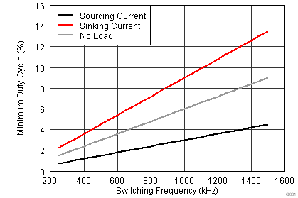 Figure 1. Ensured Minimum Duty Ratio
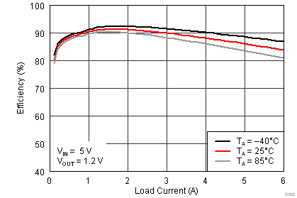 Figure 3. Efficiency, VIN = 5 V
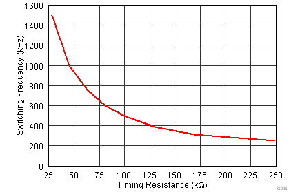 Figure 5. Switching Frequency
vs Timing Resistance (RT)
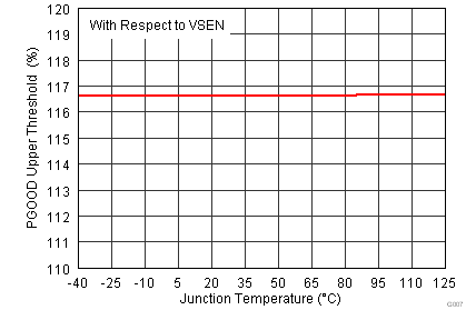 Figure 7. PGOOD Upper Threshold
vs Junction Temperature
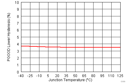 Figure 9. PGOOD Lower Hysteresis
vs Junction Temperature
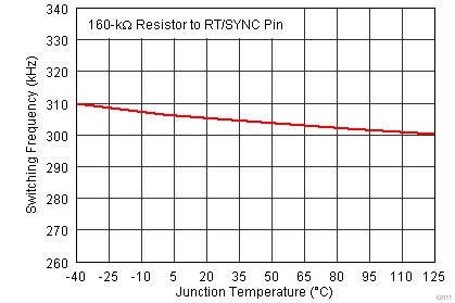 Figure 11. Switching Frequency vs Junction Temperature
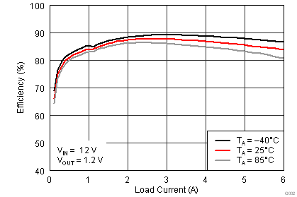 Figure 2. Efficiency, VIN = 12 V
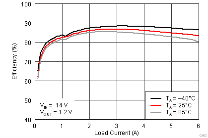 Figure 4. Efficiency, VIN = 14 V
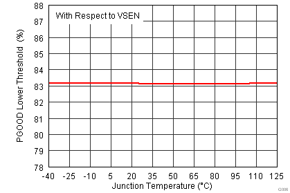 Figure 6. PGOOD Lower Threshold
vs Junction Temperature
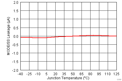 Figure 8. MODE/SS Leakage Current
vs Junction Temperature
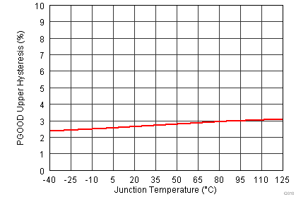 Figure 10. PGOOD Upper Hysteresis
vs Junction Temperature
7 Detailed Description
7.1 Overview
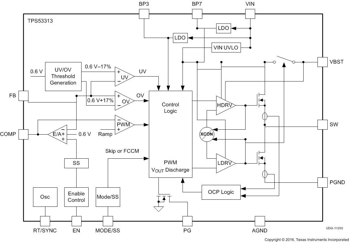
The TPS53313 is a high-efficiency switching regulator with two integrated N-channel MOSFETs and is capable of delivering up to 6 A of load current. The TPS53316 provides output voltage from 0.6 V up to 0.7 × VIN from
4.5-V to 16-V wide input voltage range. The output voltage accuracy is better than ±1% over load, line, and temperature.
This device can operate in either forced continuous conduction mode (FCCM) or skip mode with selectable soft-start time to fit various application needs. Skip mode operation provides reduced power loss and increases the efficiency at light load. The unique, patented PWM modulator enables smooth light load to heavy load transition while maintaining fast load transient.
7.2 Functional Block Diagram
7.3 Feature Description
7.3.1 Soft-Start Operation
The soft-start operation reduces the inrush current during the start-up time. A slow rising reference is generated by the soft-start circuitry and sent to the input of the error amplifier. When the soft-start ramp voltage is less than 600 mV, the error amplifier uses this ramp voltage as the reference. When the ramp voltage reaches 600 mV, a fixed 600-mV reference voltage is used for the error amplifier. The soft-start time has selectable values of 1 ms, 3 ms, and 6 ms.
7.3.2 Power Good
The TPS53313 monitors the output voltage through the FB pin. If the FB voltage is within 117% and 83% of the reference voltage, the power good signal remains high. If the FB voltage is outside of this range, the PG pin pin is pulled low by the internal open drain output.
During start up, the power good signal has a 200-µs delay after the FB voltage falls into the power good range limit when the soft-start time is set to 1 ms. There is also 10-µs delay during shut down.
7.3.3 UVLO Function
The TPS53313 provides UVLO protection for input voltage, VIN. If the input voltage is lower than UVLO threshold voltage minus the hysteresis, the device shut off. When the voltage rises above the threshold voltage, the device restarts. The typical UVLO rising threshold is 4.23 V. Hysteresis of 200 mV for input voltage is provided to prevent glitch.
7.3.4 Overcurrent (OC) Protection
The TPS53313 provides peak current protection and continuously monitors the current flowing through high-side and low-side MOSFETs. If the current through the high-side FET exceeds the current limit threshold, the high-side FET turns off and the low-side FET turns on. An overcurrent (OC) counter starts to increment every switching cycle to count the occurrence of the overcurrent events. The converter shuts down immediately when the OC counter reaches 4. The OC counter resets if the detected current is less than 6 A (with 6-A OC setting) after an OC event.
Another set of overcurrent circuitry monitors the current through low-side FET. If the current through the low-side FET exceeds 6 A (with 6-A OC setting), the overcurrent protection is engaged and turns off both high-side and low-side FETs immediately.
Therefore, the device is fully protected against overcurrent during both on-time and off-time. Also, the OC threshold is selectable and can be set to 4.5 A, 6 A, or 9 A by connecting different capacitor in parallel with MODE/SS pin. After OC events, the device stops switching and enters hiccup mode. A re-start is attempted after a hiccup waiting time. If the fault condition is not cleared, hiccup mode operation may continue indefinitely
7.3.5 Overvoltage and Undervoltage Protection
The TPS53313 monitors the voltage divided feedback voltage to detect the overvoltage and undervoltage conditions. When the feedback voltage is greater than 117% of the reference, overvoltage protection is triggered, the high-side MOSFET turns off and the low-side MOSFET turns on. Then the output voltage drops and the FB voltage reaches the undervoltage threshold. At that point the low-side MOSFET turns off and the device goes into tri-state logic.
When the feedback voltage is lower than 83% of the reference voltage, the undervoltage protection counter starts. If the feedback voltage remains lower than the undervoltage threshold voltage after 10 µs, the device turns off both the high-side and low-side MOSFETs and then goes into tri-state logic.
After the undervoltage events, the device stops switching and enters hiccup mode. A restart is attempted after a hiccup waiting time. If the fault condition is not cleared, hiccup mode operation may continue indefinitely.
7.3.6 Overtemperature Protection
The TPS53313 continuously monitors the die temperature. If the die temperature exceeds the threshold value (140°C typical), the device shuts off. When the device is cooled to 40°C below the overtemperature threshold, it restarts and returns to normal operation.
7.3.7 Output Discharge
When the EN pin is low, the TPS53313 discharges the output capacitors through an internal MOSFET switch between SW and GND while the high-side and low-side MOSFETs are maintained in the OFF state. The typical discharge switch on resistance is 120 Ω. This function is disabled when VVIN is less than 1 V.
7.3.8 Switching Frequency Setting and Synchronization
The clock frequency is programmed by the value of the resistor connected from the RT/SYNC pin to GND. The switching frequency is programmable between 250 kHz and 1.5 MHz.
Also, TPS53313 is able to synchronize to external clock. The synchronization is fulfilled by connecting the RT/SYNC pin to external clock source. If no external pulse is received from RT/SYNC pin, the device continues to operate the internal clock.
7.4 Device Functional Modes
7.4.1 Operation Mode
The TPS53313 has 6 operation modes determined by the MODE/SS pin connection as listed in Table 1. The current limit thresholds and associated capacitance selections are shown in Table 2.
Table 1. Operation Mode Selection
| MODE/SS PIN CONNECTION | OPERATION MODE | tSS SOFT-START TIME (ms) |
|---|---|---|
| 10 kΩ to GND | FCCM | 6 |
| 20 kΩ to GND | FCCM | 3 |
| 39 kΩ to GND | FCCM | 1 |
| 82 kΩ to GND | Skip mode | 6 |
| 160 kΩ to GND | Skip mode | 3 |
| Floating | Skip mode | 1 |
Table 2. Capacitor Selection
| MODE/SS PIN SETTING (nF) | CURRENT LIMIT THRESHOLD (A) |
|---|---|
| No capacitor | 6 |
| 2.2 | 4.5 |
| 10 | 9 |
In forced continuous conduction mode (FCCM), the high-side FET is ON during the on-time and low-side FET is ON during the off-time. The switching is synchronized to the internal clock thus the switching frequency is fixed.
In this mode, the switching frequency remains constant over the entire load range which is suitable for applications that need tight control of switching frequency.
In skip mode, the high-side FET is on during the on-time and low-side FET is on during the off-time until the inductor current reaches zero. An internal zero-crossing comparator detects the zero crossing of inductor current from positive to negative. When the inductor current reaches zero, the comparator sends a signal to the logic control and turns off the low-side FET. The on-pulse in skip mode is designed to be 25% higher than CCM to provide hysteresis to avoid chattering between CCM and skip mode.
Also, the overcurrent protection threshold can be set to 4.5 A, 6 A or 9 A by changing the capacitor that is in parallel with MODE/SS pin. Specifically, a 6-A current limit threshold is set without an external capacitor, the 4.5 A current limit threshold is set with a 2.2-nF capacitor, and the 9-A current limit threshold is set when a 10-nF capacitor is in parallel with MODE/SS pin.
7.4.2 Light Load Operation
In skip mode, when the load current is less than half of inductor ripple current, the inductor current reaches zero by the end of OFF-Time. The light load control scheme then turns off the low-side MOSFET when inductor current reaches zero. Since there is no negative inductor current, the energy delivered to the load per switching cycle is increased compared to the normal PWM mode operation. The controller then reduces the switching frequency to maintain the output voltage regulation. The switching loss is reduced and thus efficiency is improved.
In skip mode, when the load current decreases, the switching frequency also decreases continuously in discontinuous conduction mode (DCM). When the load current is 0 A, the minimum switching frequency is reached. It is also required that the difference between VVBST and VSW to be higher than 3.3 V to ensure the supply for high-side gate driver.
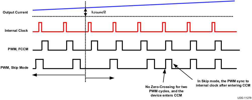 Figure 12. TPS53313 Operation Modes in Light and Heavy Load Conditions
7.4.3 Forced Continuous Conduction Mode
When choosing FCCM, the TPS53313 is operating in continuous conduction mode in both light and heavy load condition. In this mode, the switching frequency remains constant over the entire load range which is suitable for applications need tight control of switching frequency at a cost of lower efficiency at light load.