-
LMX2571 低功耗、高性能 PLLatinum RF 合成器,采用 FSK 调制
- 1 特性
- 2 应用
- 3 说明
- 4 修订历史记录
- 5 Pin Configuration and Functions
- 6 Specifications
-
7 Detailed Description
- 7.1 Overview
- 7.2 Functional Block Diagram
- 7.3
Feature Description
- 7.3.1 Reference Oscillator Input
- 7.3.2 R-Dividers and Multiplier
- 7.3.3 PLL Phase Detector and Charge Pump
- 7.3.4 PLL N-Divider and Fractional Circuitry
- 7.3.5 Partially Integrated Loop Filter
- 7.3.6 Low-Noise, Fully Integrated VCO
- 7.3.7 External VCO Support
- 7.3.8 Programmable RF Output Divider
- 7.3.9 Programmable RF Output Buffer
- 7.3.10 Integrated TX, RX Switch
- 7.3.11 Powerdown
- 7.3.12 Lock Detect
- 7.3.13 FSK Modulation
- 7.3.14 FastLock
- 7.3.15 Register Readback
- 7.4 Device Functional Modes
- 7.5 Programming
- 7.6
Register Maps
- 7.6.1 R60 Register (offset = 3Ch) [reset = 4000h]
- 7.6.2 R58 Register (offset = 3Ah) [reset = C00h]
- 7.6.3 R53 Register (offset = 35h) [reset = 2802h]
- 7.6.4 R47 Register (offset = 2Fh) [reset = 0h]
- 7.6.5 R42 Register (offset = 2Ah) [reset = 210h]
- 7.6.6 R41 Register (offset = 29h) [reset = 810h]
- 7.6.7 R40 Register (offset = 28h) [reset = 101Ch]
- 7.6.8 R39 Register (offset = 27h) [reset = 11F0h]
- 7.6.9 R35 Register (offset = 23h) [reset = 647h]
- 7.6.10 R34 Register (offset = 22h) [reset = 1000h]
- 7.6.11 R33 Register (offset = 21h) [reset = 0h]
- 7.6.12 R25 to R32 Register (offset = 19h to 20h) [reset = 0h]
- 7.6.13 R24 Register (offset = 18h) [reset = 10h]
- 7.6.14 R23 Register (offset = 17h) [reset = 10A4h]
- 7.6.15 R22 Register (offset = 16h) [reset = 8584h]
- 7.6.16 R21 Register (offset = 15h) [reset = 101h]
- 7.6.17 R20 Register (offset = 14h) [reset = 28h]
- 7.6.18 R19 Register (offset = 13h) [reset = 0h]
- 7.6.19 R18 Register (offset = 12h) [reset = 0h]
- 7.6.20 R17 Register (offset = 11h) [reset = 0h]
- 7.6.21 R9 to R16 Register (offset = 9h to 10h) [reset = 0h]
- 7.6.22 R8 Register (offset = 8h) [reset = 10h]
- 7.6.23 R7 Register (offset = 7h) [reset = 10A4h]
- 7.6.24 R6 Register (offset = 6h) [reset = 8584h]
- 7.6.25 R5 Register (offset = 5h) [reset = 101h]
- 7.6.26 R4 Register (offset = 4h) [reset = 28h]
- 7.6.27 R3 Register (offset = 3h) [reset = 0h]
- 7.6.28 R2 Register (offset = 2h) [reset = 0h]
- 7.6.29 R1 Register (offset = 1h) [reset = 0h]
- 7.6.30 R0 Register (offset = 0h) [reset = 3h]
-
8 Application and Implementation
- 8.1
Application Information
- 8.1.1 Direct Digital FSK Modulation
- 8.1.2 Frequency and Output Port Switching with TrCtl Pin
- 8.1.3 OSCin Configuration
- 8.1.4 Register R0 F1F2_INIT, F1F2_MODE usage
- 8.1.5 FastLock with External VCO
- 8.1.6 OSCin Slew Rate
- 8.1.7 RF Output Buffer Power Control
- 8.1.8 RF Output Buffer Type
- 8.1.9 MULT Multiplier
- 8.1.10 Integrated VCO
- 8.2 Typical Applications
- 8.3 Do's and Don'ts
- 8.1
Application Information
- 9 Power Supply Recommendations
- 10Layout
- 11器件和文档支持
- 12机械封装和可订购信息
- 重要声明
DATA SHEET
LMX2571 低功耗、高性能 PLLatinum RF 合成器,采用 FSK 调制
本资源的原文使用英文撰写。 为方便起见,TI 提供了译文;由于翻译过程中可能使用了自动化工具,TI 不保证译文的准确性。 为确认准确性,请务必访问 ti.com 参考最新的英文版本(控制文档)。
1 特性
- 输出频率范围:10MHz 至 1344MHz
- 低相位噪声和毛刺
- 12.5kHz 偏移 @ 480MHz 时为 –123dBc/Hz
- 1MHz 偏移 @ 480MHz 时为 –145dBc/Hz
- 标准化锁相环 (PLL) 噪底为 –231dBc/Hz
- 杂散优于 –75dBc/Hz
- 新型 FastLock 技术,缩短了锁定时间
- 新型整数边界毛刺去除技术
- 集成 5V 电荷泵和输出驱动器,用于外部压控振荡器 (VCO) 操作
- 2、4 和 8 电平或者任意电平数直接数字移频键控 (FSK) 调制
- 一个 TX/RX 输出或两个扇出输出
- 晶振、XO 或差分参考时钟输入
- 低电流消耗
- 39mA 典型合成器模式(内部 VCO)
- 9mA 典型 PLL 模式(外部 VCO)
- 24 位分数 N Δ-Σ 调制器
2 应用
- 双工模式数字专业双向无线电
- dPMR、DMR、PDT、P25 Phase I
- 低功耗无线电通信系统
- 卫星通信调制解调器
- 无线麦克风
- 专有无线连接
- 手持式测试和测量设备
3 说明
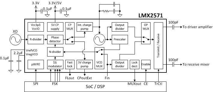
LMX2571 是一款低功耗、高性能、宽带 PLLatinum™ 射频 (RF) 合成器,该合成器集成了 Δ-Σ 分数 N PLL、多核压控振荡器 (VCO)、可编程输出分压器以及两个输出缓冲器。 VCO 内核的工作频率高达 5.376GHz,持续输出频率范围为 10MHz 至 1344MHz。
该合成器还可搭配外部 VCO 使用。 在此配置下,需使用专用的 5V 电荷泵和输出分压器。
该合成器还包含一个独特的可编程乘法器,有助于去除毛刺,即使毛刺落在整数边界,系统也仍能够使用任一通道。
其输出具有 SPDT 开关,可用作 FDD 无线电应用中的发送/接收开关。 并且可同时导通两个开关,以便同时提供双输出。
LMX2571 通过编程或相应引脚来支持直接数字 FSK 调制。 该器件支持离散电平 FSK、脉冲成形 FSK 以及模拟 FM 调制。
该器件采用了一项全新的 FastLock 技术,即使在外部 VCO 与窄带回路滤波器搭配使用时,用户也能够在不到 1.5ms 的时间内从一个频率切换至另一频率。
器件信息(1)
| 器件型号 | 封装 | 封装尺寸(标称值) |
|---|---|---|
| LMX2571 | WQFN (36) | 6.00mm x 6.00mm |
- 如需了解所有可用封装,请见数据表末尾的可订购产品附录。
4 修订历史记录
| 日期 | 修订版本 | 注释 |
|---|---|---|
| 2015 年 3 月 | * | 最初发布。 |
5 Pin Configuration and Functions
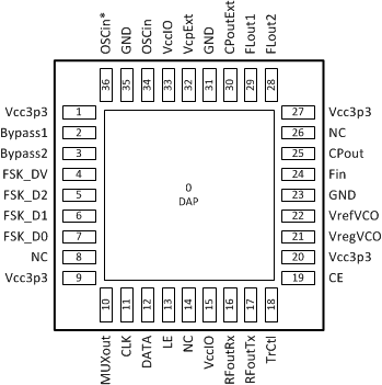
WQFN (NJK) Package
36 Pins
Top View
Pin Functions
| PIN | TYPE | DESCRIPTION | |
|---|---|---|---|
| NAME | NO. | ||
| Bypass1 | 2 | Bypass | Place a 100-nF capacitor to GND. |
| Bypass2 | 3 | Bypass | Place a 100-nF capacitor to GND. |
| CE | 19 | Input | Chip Enable input. Active HIGH powers on the device. |
| CLK | 11 | Input | MICROWIRE clock input. |
| CPout | 25 | Output | Internal VCO charge pump access point to connect to a 2nd order loop filter. |
| CPoutExt | 30 | Output | 5-V charge pump output used in PLL mode (external VCO). |
| DAP | 0 | GND | The DAP should be grounded. |
| DATA | 12 | Input | MICROWIRE serial data input. |
| Fin | 24 | Input | High frequency AC coupled input pin for an external VCO. Leave it open or AC coupled to GND if not being used. |
| FSK_D0 | 7 | Input | FSK data bit 0 (FSK PIN mode) / I2S FS input (FSK I2S mode). |
| FSK_D1 | 6 | Input | FSK data bit 1 (FSK PIN mode) / I2S DATA input (FSK I2S mode). |
| FSK_D2 | 5 | Input | FSK data bit 2 (FSK PIN mode). |
| FSK_DV | 4 | Input | FSK data valid input (FSK PIN mode) / I2S CLK input (FSK I2S mode). |
| FLout1 | 29 | Output | FastLock output control 1 for external switch. Output is HIGH when F1 is selected. |
| FLout2 | 28 | Output | FastLock output control 2 for external switch. Output is HIGH when F2 is selected. |
| GND | 23 | GND | VCO ground. |
| GND | 31 | GND | Charge pump ground. |
| GND | 35 | GND | OSCin ground. |
| LE | 13 | Input | MICROWIRE latch enable input. |
| MUXout | 10 | Output | Multiplexed output that can be assigned to lock detect or readback serial data output. |
| NC | 8,14, 26 | NC | Do not connect these pins. |
| OSCin | 34 | Input | Reference clock input. |
| OSCin* | 36 | Input | Complementary reference clock input. |
| RFoutRx | 16 | Output | RF output used to drive receive mixer. Selectable open drain or push-pull output. |
| RFoutTx | 17 | Output | RF output used to drive transmit signal. Selectable open drain or push-pull output. |
| TrCtl | 18 | Input | Transmit/Receive control. This pin controls the RF output port and the output frequency selection. |
| Vcc3p3 | 1, 9, 20, 27 | Supply | Connect to 3.3-V supply. |
| VccIO | 15, 33 | Supply | Supply for digital logic interface. Connect to 3.3-V supply. |
| VcpExt | 32 | Supply | Supply for 5-V charge pump. Connect to 5-V supply in PLL mode. Connect to either 3.3-V or 5-V supply in synthesizer mode. |
| VrefVCO | 22 | Bypass | LDO output. Place a 100-nF capacitor to GND. |
| VregVCO | 21 | Bypass | Bias circuitry for the VCO. Place a 2.2-µF capacitor to GND. |
6 Specifications
6.1 Absolute Maximum Ratings
Over operating free-air temperature range (unless otherwise noted) (1)| MIN | MAX | UNIT | ||
|---|---|---|---|---|
| VCC | Power supply voltage | –0.3 | 3.6 | V |
| VIO | IO supply voltage | –0.3 | 3.6 | V |
| VIN | IO input voltage | VCC + 0.3 | V | |
| VCP | Charge pump supply voltage | 5.25 | V | |
| TJ | Junction temperature | 150 | °C | |
| TSTG | Storage temperature | –65 | 150 | °C |
(1) Stresses beyond those listed under Absolute Maximum Ratings may cause permanent damage to the device. These are stress ratings only, which do not imply functional operation of the device at these or any other conditions beyond those indicated under Recommended Operating Conditions. Exposure to absolute-maximum-rated conditions for extended periods may affect device reliability.
6.2 ESD Ratings
| VALUE | UNIT | |||
|---|---|---|---|---|
| V(ESD) | Electrostatic discharge | Human-body model (HBM), per ANSI/ESDA/JEDEC JS-001(1) | ±1500 | V |
| Charged-device model (CDM), per JEDEC specification JESD22-C101(2) | ±500 | |||
(1) JEDEC document JEP155 states that 500-V HBM allows safe manufacturing with a standard ESD control process.
(2) JEDEC document JEP157 states that 250-V CDM allows safe manufacturing with a standard ESD control process.
6.3 Recommended Operating Conditions
Over operating free-air temperature range (unless otherwise noted)| MIN | MAX | UNIT | |||
|---|---|---|---|---|---|
| VCC | Power supply voltage | 3.15 | 3.45 | V | |
| VIO | IO supply voltage | VCC | V | ||
| VCP | Charge pump supply voltage | PLL mode (external VCO) | 5 | V | |
| Synthesizer mode (internal VCO) | VCC | 5 | |||
| TA | Ambient temperature | –40 | 85 | °C | |
| TJ | Junction Temperature | 125 | °C | ||
6.4 Thermal Information
| THERMAL METRIC(1) | LMX2571 | UNIT | |
|---|---|---|---|
| WQFN (NJK) | |||
| 36 PINS | |||
| RθJA | Junction-to-ambient thermal resistance | 32.9 | °C/W |
| RθJC(top) | Junction-to-case (top) thermal resistance | 14.5 | |
| RθJB | Junction-to-board thermal resistance | 6.3 | |
| ψJT | Junction-to-top characterization parameter | 0.2 | |
| ψJB | Junction-to-board characterization parameter | 6.3 | |
| RθJC(bot) | Junction-to-case (bottom) thermal resistance | 2.0 | |
(1) For more information about traditional and new thermal metrics, see the IC Package Thermal Metrics application report, SPRA953.
6.5 Electrical Characteristics
3.15 V ≤ VCC ≤ 3.45 V, VIO = VCC, –40 °C ≤ TA ≤ 85 °C, except as specified. Typical values are at VCC = VIO = 3.3 V, VCP = 3.3 V or 5 V in synthesizer mode, VCP = 5 V in PLL mode, TA = 25 °C.| PARAMETER | TEST CONDITIONS | MIN | TYP | MAX | UNIT | ||
|---|---|---|---|---|---|---|---|
| CURRENT CONSUMPTION | |||||||
| ICC | Total current in synthesizer mode (internal VCO) | fOUT = 480 MHz SE OSCin |
Configuration A(1) | 39 | mA | ||
| Configuration B(2) | 44 | ||||||
| Configuration C(3) | 46 | ||||||
| Configuration D(4) | 51 | ||||||
| IPLL | Total current in PLL mode (external VCO) | Configuration E(5) | 9 | ||||
| Configuration F(6) | 15 | ||||||
| Configuration G(7) | 21 | ||||||
| ICCPD | Power down current | CE = 0V or POWERDOWN bit = 1 VCC = 3.3 V, Push-pull output |
0.9 | ||||
| OSCIN REFERENCE INPUT | |||||||
| fOSCin | OSCin frequency range | Single-ended or differential input | 10 | 150 | MHz | ||
| VOSCin | OSCin input voltage(8) | Single-ended input | 1.4 | 3.3 | V | ||
| Differential input | 0.15 | 1.5 | |||||
| CRYSTAL REFERENCE INPUT | |||||||
| fXTAL | Crystal frequency range | Fundamental model, ESR < 200 Ω | 10 | 40 | MHz | ||
| CIN | OSCin input capacitance | 1 | pF | ||||
| MULT | |||||||
| fMULTin | MULT input frequency | MULT > Pre-divider Not supported with crystal reference input |
10 | 30 | MHz | ||
| fMULTout | MULT output frequency | 60 | 130 | MHz | |||
| PLL | |||||||
| fPD | Phase detector frequency | 130 | MHz | ||||
| KPD | Charge pump current(9) | Programmable minimum value | Internal charge pump | 312.5 | µA | ||
| 5-V charge pump | 625 | ||||||
| Per programmable step | Internal charge pump | 312.5 | |||||
| 5-V charge pump | 625 | ||||||
| Programmable maximum value | Internal charge pump | 7187.5 | |||||
| 5-V charge pump | 6875 | ||||||
| PNPLL_1/f | Normalized PLL 1/f noise(10) | At maximum charge pump current | Internal charge pump | –124 | dBc/Hz | ||
| 5-V charge pump | –120 | ||||||
| PNPLL_Flat | Normalized PLL noise floor(10) | Internal charge pump | –231 | dBc/Hz | |||
| 5-V charge pump | –226 | ||||||
| fRFin | External VCO input frequency | 100 | 1400 | MHz | |||
| PRFin | External VCO input power | fRFin < 1 GHz | –10 | dBm | |||
| fRFin ≥ 1 GHz | –5 | ||||||
| VCO | |||||||
| fVCO | VCO frequency | 4300 | 5376 | MHz | |||
| KVCO | VCO gain(11) | fVCO = 4800 MHz | 56 | MHz/V | |||
| | ΔTCL | | Allowable temperature drift(12) | VCO not being re-calibrated, –40 °C ≤ TA ≤ 85 °C | 125 | °C | |||
| tVCOCal | VCO calibration time | fOSCin = fPD = 100 MHz | 140 | µs | |||
| PNVCO | Open loop VCO phase noise | fOUT = 480 MHz | 100 Hz offset | –32.4 | dBc/Hz | ||
| 1 kHz offset | –62.3 | ||||||
| 10 kHz offset | –92.1 | ||||||
| 100 kHz offset | –121.1 | ||||||
| 1 MHz offset | –144.5 | ||||||
| 10 MHz offset | –156.8 | ||||||
| RF OUTPUT | |||||||
| fOUT | RF output frequency | Synthesizer mode | 10 | 1344 | MHz | ||
| PLL mode, RF output from buffer | 10 | 1400 | |||||
| PTX, PRX | RF output power | fOUT = 480 MHz | Power control bit = 6 | 0 | dBm | ||
| H2RFout | Second harmonic | –25 | dBc | ||||
| DIGITAL FSK MODULATION | |||||||
| FSKLevel | FSK level(13) | FSK PIN mode | 2 | 8 | |||
| FSKBaud | FSK baud rate(14) | Loop bandwidth = 200 kHz | 100 | kSPs | |||
| FSKDev | FSK deviation | Configuration H(15) | ±39 | kHz | |||
| DIGITAL INTERFACE | |||||||
| VIH | High level input voltage | 1.4 | VIO | V | |||
| VIL | Low level input voltage | 0.4 | V | ||||
| IIH | High level input current | VIH = 1.75 V | –25 | 25 | µA | ||
| IIL | Low level input current | VIL = 0 V | –25 | 25 | µA | ||
| VOH | High level output voltage | IOH = 500 µA | 2 | V | |||
| VOL | Low level output voltage | IOL = –500 µA | 0 | 0.4 | V | ||
(1) fOSCin = 19.44 MHz, MULT = 1, Prescaler = 4, fPD = 19.44 MHz, one RF output, output type = push pull, output power = –3 dBm
(2) fOSCin = 19.44 MHz, MULT = 1, Prescaler = 2, fPD = 19.44 MHz, one RF output, output type = push pull, output power = –3 dBm
(3) fOSCin = 19.44 MHz, MULT = 5, Prescaler = 2, fPD = 19.44 MHz, one RF output, output type = push pull, output power = –3 dBm
(4) fOSCin = 19.44 MHz, MULT = 5, Prescaler = 2, fPD = 97.2 MHz, one RF output, output type = push pull, output power = –3 dBm
(5) fOSCin = 19.44 MHz, MULT = 1, fPD = 19.44 MHz, output from VCO
(6) fOSCin = 19.44 MHz, MULT = 1, fPD = 19.44 MHz, one RF output, output type = push pull, output power = –3 dBm
(7) fOSCin = 19.44 MHz, MULT = 1, fPD = 19.44 MHz, two RF outputs, output type = push pull, output power = –3 dBm
(8) See OSCin Configuration for definition of OSCin input voltage.
(9) This is referring to the total base charge pump current. In PLL mode, this is equal to EXTVCO_CP_IDN + EXTVCO_CP_IUP. In synthesizer mode, this is equal to CP_IDN + CP_IUP. See Table 5, Table 6 and Table 7 for details.
(10) Measured with a clean OSCin signal with a high slew rate using a wide loop bandwidth. The noise metrics model the PLL noise for an infinite loop bandwidth as:
PLL_Total = 10 * log[10(PLL_Flat / 10) + 10(PLL_Flicker / 10)]
PLL_Flat = PN1Hz + 20 * log(N) + 10 * log(fPD)
PLL_Flicker = PN10kHz – 10 * log(Offset / 10 kHz) + 20 * log(fOUT / 1 GHz)
PLL_Total = 10 * log[10(PLL_Flat / 10) + 10(PLL_Flicker / 10)]
PLL_Flat = PN1Hz + 20 * log(N) + 10 * log(fPD)
PLL_Flicker = PN10kHz – 10 * log(Offset / 10 kHz) + 20 * log(fOUT / 1 GHz)
(11) The VCO gain changes as a function of the VCO core and frequency. See Integrated VCO for details.
(12) Not tested in production. Ensured by characterization. Allowable temperature drift refers to programming the device at an initial temperature and allowing this temperature to drift WITHOUT reprogramming the device, and still have the device stay in lock. This change could be up or down in temperature and the specification does not apply to temperatures that go outside the recommended operating temperatures of the device.
(13) The data showed here simply specifies the range of discrete FSK level that is supported in PIN mode. PIN mode supports 2-, 4- and 8-level of FSK modulation. If arbitrary level of FSK modulation is desired, use FSK SPI™ FAST mode or FSK I2S mode. See Direct Digital FSK Modulation for details.
(14) The baud rate is limited by the loop bandwidth of the PLL loop. As a general rule of thumb, it is desirable to have the loop bandwidth at least twice the baud rate.
(15) fPD = 100 MHz, DEN = 224, CHDIV1 = 5, CHDIV2 = 2, Prescaler = 2, FSK step value = 32716, 32819. The maximum achievable frequency deviation depends on the configuration, see Direct Digital FSK Modulation for details.
6.6 Timing Requirements
3.15 V ≤ VCC ≤ 3.45 V, VIO = VCC, –40 °C ≤ TA ≤ 85 °C, except as specified. Typical values are at VCC = VIO = 3.3 V, TA = 25 °C.| MIN | NOM | MAX | UNIT | |||
|---|---|---|---|---|---|---|
| MICROWIRE TIMING | ||||||
| tES | Clock to enable low time | See Figure 1 | 5 | ns | ||
| tCS | Data to clock setup time | 2 | ns | |||
| tCH | Data to clock hold time | 2 | ns | |||
| tCWH | Clock pulse width high | 5 | ns | |||
| tCWL | Clock pulse width low | 5 | ns | |||
| tCES | Enable to clock setup time | 5 | ns | |||
| tEWH | Enable pulse width high | 2 | ns | |||
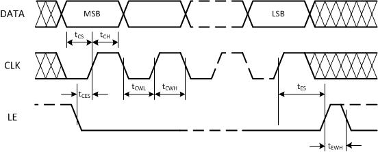 Figure 1. MICROWIRE Timing Diagram
There are several other considerations for programming:
- A slew rate of at least 30 V/µs is recommended for the CLK, DATA and LE. The same apply for other digital control signals such as FSK_D[0:2] and FSK_DV signals.
- The DATA is clocked into a shift register on each rising edge of the CLK signal. On the rising edge of the LE signal, the data is sent from the shift register to an active register.
- The LE pin may be held high after programming, causing the LMX2571 to ignore clock pulses.
- When CLK or DATA lines are shared between devices, it is recommended to divide down the voltage to the CLK, DATA, and LE pins closer to the minimum voltage. This provides better noise immunity.
- If the CLK and DATA lines are toggled while the VCO is in lock, as is sometimes the case when these lines are shared with other parts, the phase noise may be degraded during the time of this programming.
6.7 Typical Characteristics
At TA = 25 °C, unless otherwise noted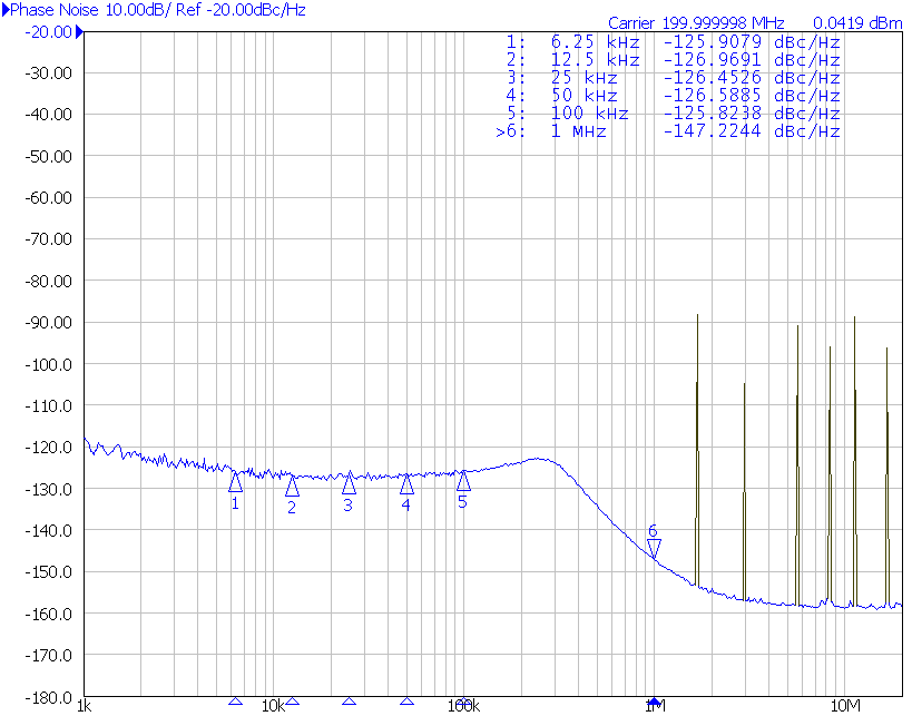
| OSCin = 19.44 MHz | fOUT = 200 MHz | Synthesizer mode |
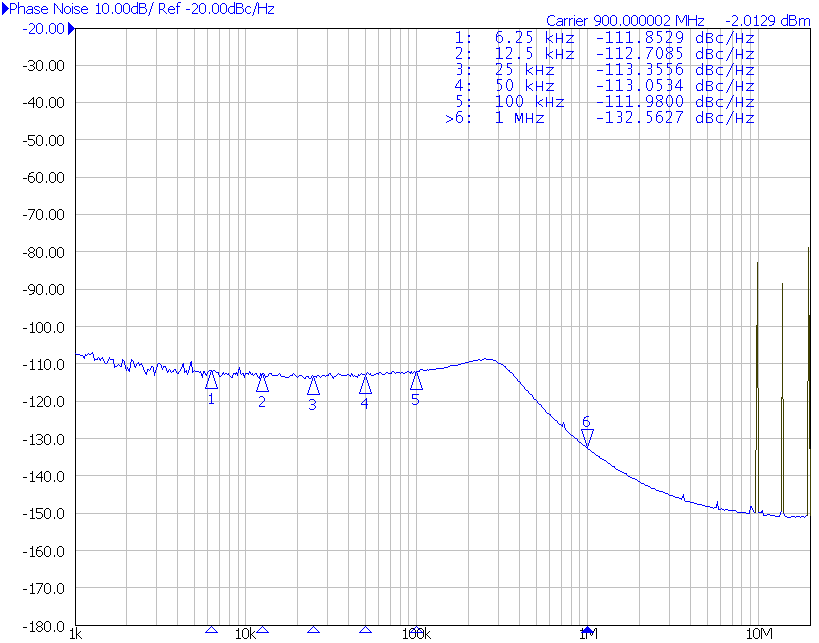
| OSCin = 19.44 MHz | fOUT = 900 MHz | Synthesizer mode |
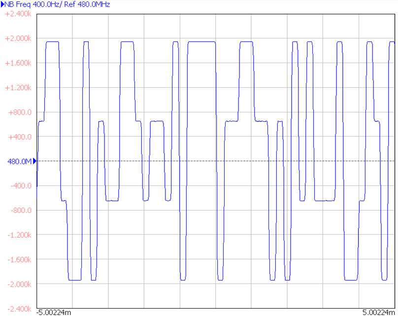
| FSKBaud = 4.8 kSPS | FSK PIN mode |
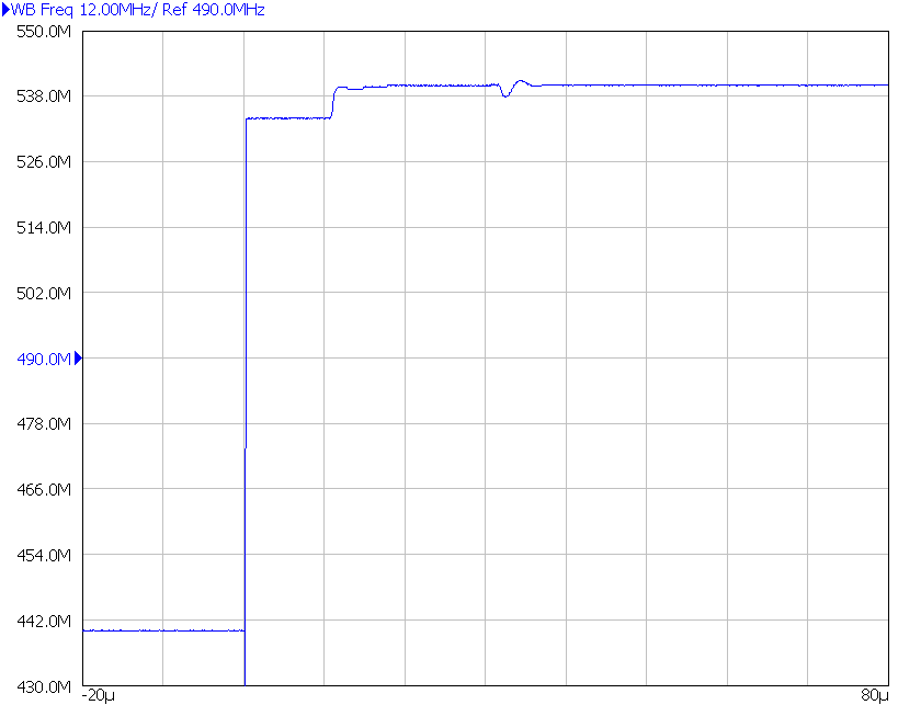
| Switching between int. and ext. VCO as well as Tx and Rx port |
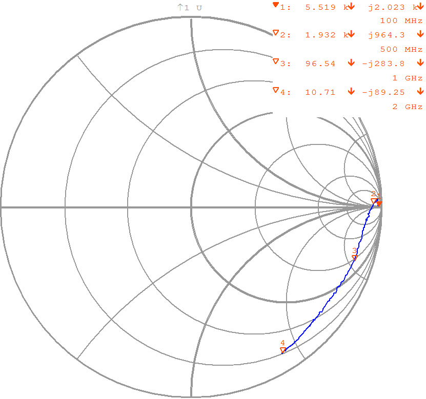
| Start: 100 MHz | Stop: 2000 MHz |
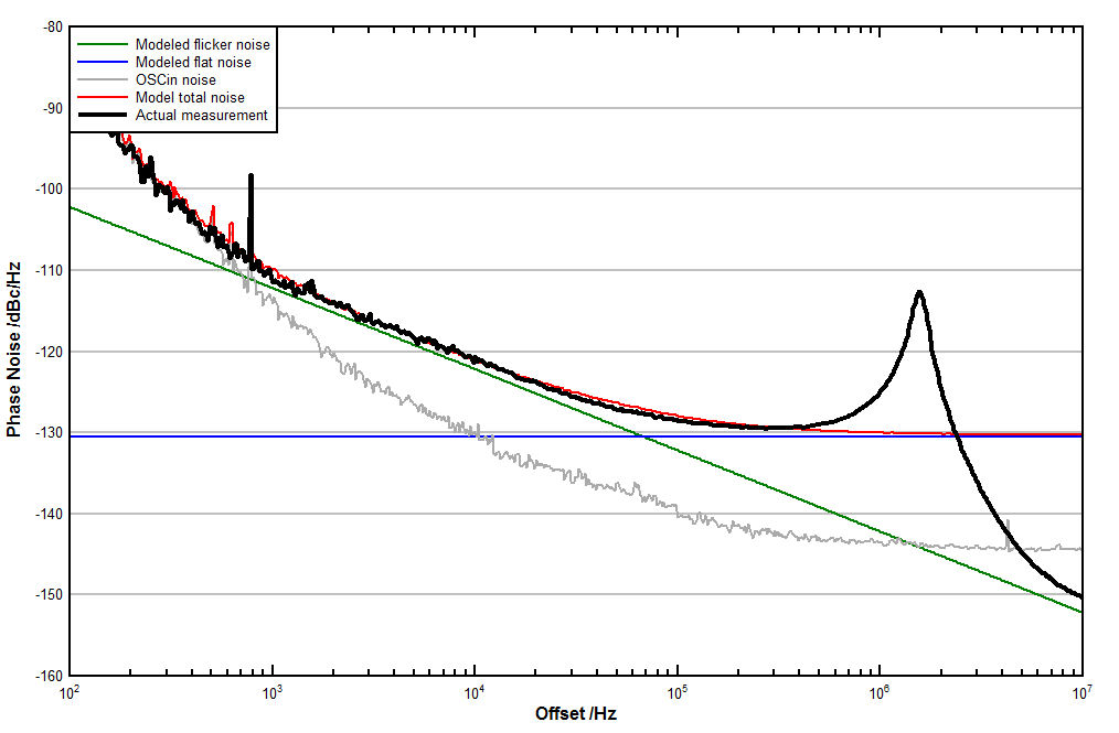
| fOUT = 1228.8 MHz | fPD = 122.88 MHz | Synthesizer mode |
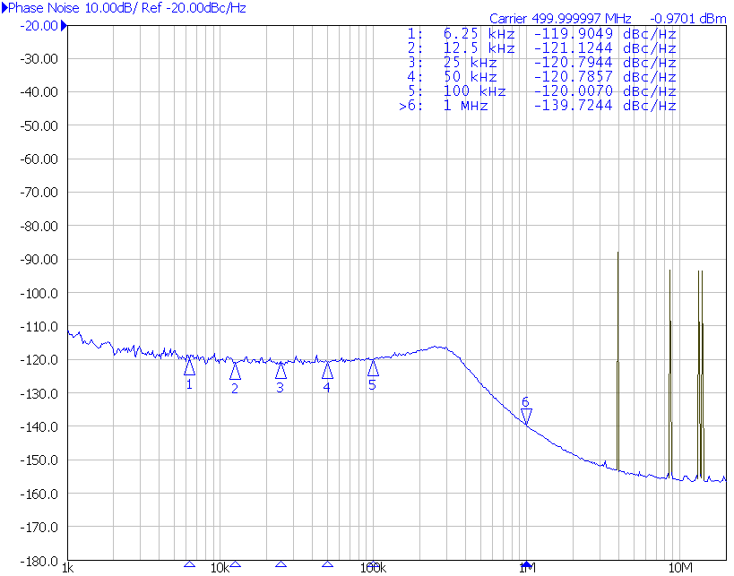
| OSCin = 19.44 MHz | fOUT = 500 MHz | Synthesizer mode |
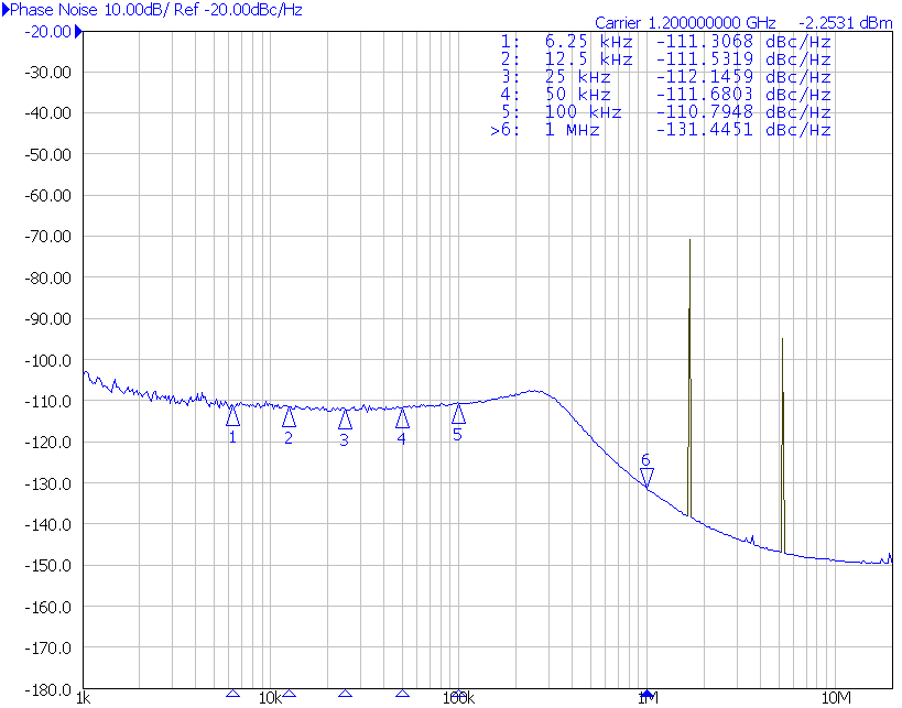
| OSCin = 19.44 MHz | fOUT = 1200 MHz | Synthesizer mode |
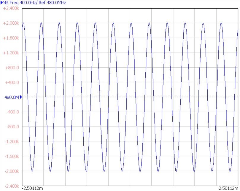
| Reference clock is a FM modulated signal with fMOD = 2.4 kHz |
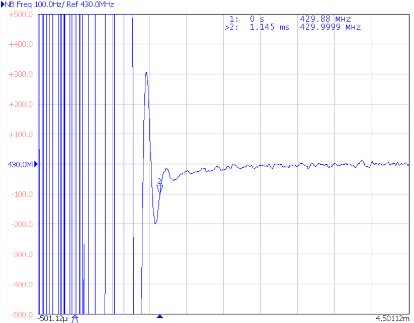
| Freq. jump = 50 MHz | LBW = 4 kHz | PLL mode |
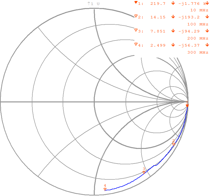
| Start: 10 MHz | Stop: 300 MHz |
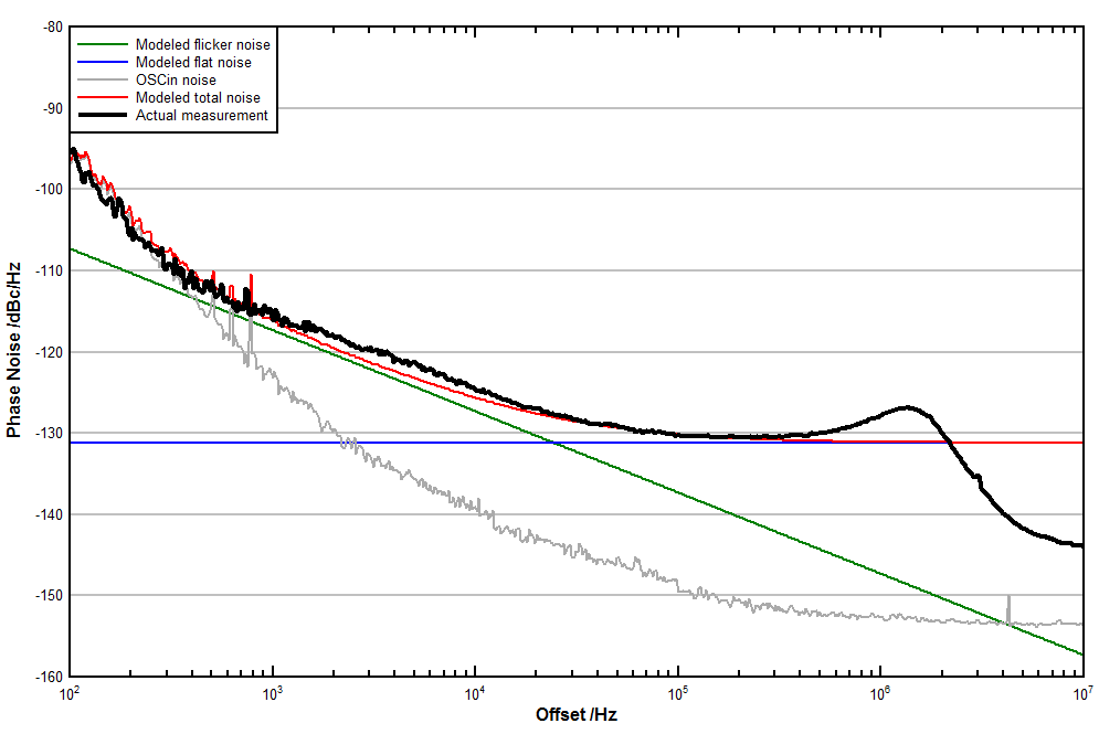
| fOUT = 430.08 MHz | fPD = 61.44 MHz | PLL mode |