-
具有集成 PGA 和基准的 ADS1120 4 通道、2kSPS、低功耗、16 位 ADC
- 1 特性
- 2 应用
- 3 说明
- 4 修订历史记录
- 5 Pin Configuration and Functions
- 6 Specifications
- 7 Parameter Measurement Information
-
8 Detailed Description
- 8.1 Overview
- 8.2 Functional Block Diagram
- 8.3 Feature Description
- 8.4 Device Functional Modes
- 8.5 Programming
- 8.6 Register Map
- 9 Application and Implementation
- 10Power Supply Recommendations
- 11Layout
- 12器件和文档支持
- 13机械、封装和可订购信息
- 重要声明
DATA SHEET
具有集成 PGA 和基准的 ADS1120 4 通道、2kSPS、低功耗、16 位 ADC
本资源的原文使用英文撰写。 为方便起见,TI 提供了译文;由于翻译过程中可能使用了自动化工具,TI 不保证译文的准确性。 为确认准确性,请务必访问 ti.com 参考最新的英文版本(控制文档)。
1 特性
- 低电流消耗:
占空比模式下低至 120μA(典型值) - 宽电源范围:2.3V 至 5.5V
- 可编程增益:1V/V 至 128V/V
- 可编程数据速率:高达 2kSPS
- 16 位无噪声分辨率(20SPS 时)
- 采用单周期稳定数字滤波器,在 20SPS 时
实现 50Hz 和 60Hz 谐波抑制 - 两个差分输入或四个单端输入
- 双匹配可编程电流源:50μA 至 1.5mA
- 内部 2.048V 基准电压:漂移 5ppm/°C(典型值)
- 集成 2% 精准振荡器
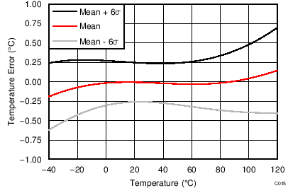
- 集成温度传感器:精度 0.5°C(典型值)
- 与 SPI 兼容的接口(模式 1)
- 封装:3.5mm × 3.5mm × 0.9mm 超薄型四方扁平无引线 (VQFN)
2 应用
- 温度传感器测量:
- 热敏电阻
- 热电偶
- 电阻式温度检测器 (RTD):
2 线、3 线或 4 线制类型
- 电阻桥式传感器测量:
- 压力传感器
- 应力计
- 衡器
- 便携式仪表
- 工厂自动化和过程控制
3 说明
ADS1120 是一款 16 位高精度模数转换器 (ADC),集成了多种 特性, 能够降低系统成本并减少小型传感器信号测量 应用 中的组件数量。该器件 具有 通过输入多路复用器 (MUX) 实现的两个差分输入或四个单端输入,一个低噪声可编程增益放大器 (PGA),两个可编程激励电流源,一个电压基准,一个振荡器,一个低侧开关和一个精密温度传感器。
此器件能够以高达 2000 次/秒 (SPS) 采样数据速率执行转换,并且能够在单周期内稳定。针对噪声环境中的工业应用,当采样频率为 20SPS 时,数字滤波器可同时提供 50Hz 和 60Hz 抑制。内部 PGA 提供高达 128V/V 的增益。此 PGA 使得 ADS1120 非常适用于小型传感器信号测量 应用 ,例如电阻式温度检测器 (RTD)、热电偶、热敏电阻和桥式传感器。该器件在使用 PGA 时支持测量伪差分或全差分信号。此外,该器件还可配置为禁用内部 PGA,同时仍提供高输入阻抗和高达 4V/V 的增益,从而实现单端测量。
在禁用 PGA 后的占空比模式下运行功耗可低至 120µA。ADS1120 采用无引线 VQFN-16 或薄型小外形尺寸 (TSSOP)-16 封装,额定工作温度范围为 -40°C 至 +125°C。
器件信息(1)
| 器件型号 | 封装 | 封装尺寸(标称值) |
|---|---|---|
| ADS1120 | VQFN (16) | 3.50mm x 3.50mm |
| TSSOP (16) | 5.00mm x 4.40mm |
- 如需了解所有可用封装,请见数据表末尾的可订购产品附录。
4 修订历史记录
Changes from B Revision (January 2015) to C Revision
- Changed 文档标题Go
- Changed K 型热电偶测量图Go
- Added footnote 1 to Pin Functions table and changed descriptions of AIN0/REFP1, AIN1, AIN2, AIN3/REFN1, REFN0, and REFP0 pins accordingly Go
- Changed format of Absolute Maximum Ratings tableGo
- Changed Functional Block Diagram figure Go
- Changed Bypassing the PGA sectionGo
- Changed (AVDD) to (AVDD – AVSS) in first paragraph of Voltage Reference sectionGo
- Added fourth sentence to Temperature Sensor sectionGo
- Changed last equation in Converting from Digital Codes to Temperature sectionGo
- Changed bit 0 in register 03h to 0 from RESERVED Go
- Changed description of bits 5:4 in Configuration Register 2Go
- Added Unused Inputs and Outputs section Go
- Changed Thermocouple Measurement figureGo
- Changed 3-Wire RTD Measurement figure Go
- Changed 2-Wire RTD Measurement figure Go
- Changed 4-Wire RTD Measurement figure Go
- Changed Resistive Bridge Measurement figure Go
- Changed Power Supply Recommendations section: changed Power-Supply Sequencing subsection, added Power-Supply Ramp Rate subsectionGo
Changes from A Revision (January 2014) to B Revision
- 增加了 ESD 额定值表、推荐的运行条件表、应用和实施、电源相关建议、布局、器件和文档支持以及机械、封装和可订购信息部分Go
- 更改了文档标题、特性, 应用, 说明,引脚配置和功能,参数测量信息,特性 说明,器件功能模式,编程,寄存器映射部分以及首页图Go
- Deleted Ordering Information section and Product Family tableGo
- Changed format of Absolute Maximum Ratings table and added minimum junction temperature specificationGo
- Changed Analog Inputs and Voltage Reference Input sections (specification values were not changed) and added Internal Oscillator section to Electrical Characteristics tableGo
- Changed System Performance section: changed VIO parameter name, deleted symbol and changed test conditions of Gain error parameter in Electrical Characteristics table Go
- Deleted Clock Sources section and changed Temperature Sensor and Power Supply sections (specification values were not changed) in Electrical Characteristics tableGo
- Changed SPI Timing Requirements and Figure 1 (specification values were not changed), added SPI Switching Characteristics and Figure 2 Go
- Changed format of Typical Characteristics section (actual curves did not change)Go
Changes from * Revision (August 2013) to A Revision
- 投入生产Go
5 Pin Configuration and Functions
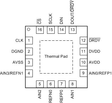
RVA Package
16-Pin VQFN
Top View
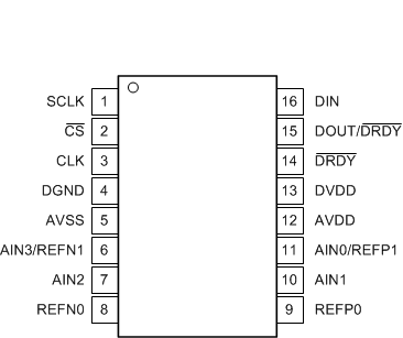
PW Package
16-Pin TSSOP
Top View
Pin Functions
| PIN | ANALOG OR DIGITAL INPUT/OUTPUT |
DESCRIPTION(1) | ||
|---|---|---|---|---|
| NAME | NO. | |||
| RVA | PW | |||
| AIN0/REFP1 | 9 | 11 | Analog input | Analog input 0, positive reference input 1 |
| AIN1 | 8 | 10 | Analog input | Analog input 1 |
| AIN2 | 5 | 7 | Analog input | Analog input 2 |
| AIN3/REFN1 | 4 | 6 | Analog input | Analog input 3, negative reference input 1. Internal low-side power switch connected between AIN3/REFN1 and AVSS. |
| AVDD | 10 | 12 | Analog | Positive analog power supply |
| AVSS | 3 | 5 | Analog | Negative analog power supply |
| CLK | 1 | 3 | Digital input | External clock source pin. Connect to DGND if not used. |
| CS | 16 | 2 | Digital input | Chip select; active low. Connect to DGND if not used. |
| DGND | 2 | 4 | Digital | Digital ground |
| DIN | 14 | 16 | Digital input | Serial data input |
| DOUT/DRDY | 13 | 15 | Digital output | Serial data output combined with data ready; active low |
| DRDY | 12 | 14 | Digital output | Data ready, active low. Leave unconnected or tie to DVDD using a weak pull-up resistor if not used. |
| DVDD | 11 | 13 | Digital | Positive digital power supply |
| REFN0 | 6 | 8 | Analog input | Negative reference input 0 |
| REFP0 | 7 | 9 | Analog input | Positive reference input 0 |
| SCLK | 15 | 1 | Digital input | Serial clock input |
| Thermal pad | — | — | Thermal power pad. Do not connect or only connect to AVSS. | |
(1) See the Unused Inputs and Outputs section for unused pin connections.
6 Specifications
6.1 Absolute Maximum Ratings(1)
(1) Stresses beyond those listed under Absolute Maximum Ratings may cause permanent damage to the device. These are stress ratings only, which do not imply functional operation of the device at these or any other conditions beyond those indicated under Recommended Operating Conditions. Exposure to absolute-maximum-rated conditions for extended periods may affect device reliability.
6.2 ESD Ratings
| VALUE | UNIT | |||
|---|---|---|---|---|
| V(ESD) | Electrostatic discharge | Human-body model (HBM), per ANSI/ESDA/JEDEC JS-001(1) |
±2000 | V |
| Charged-device model (CDM), per JEDEC specification JESD22-C101(2) |
±500 | |||
(1) JEDEC document JEP155 states that 500-V HBM allows safe manufacturing with a standard ESD control process..
(2) JEDEC document JEP157 states that 250-V CDM allows safe manufacturing with a standard ESD control process.
6.3 Recommended Operating Conditions
over operating ambient temperature range (unless otherwise noted)| MIN | NOM | MAX | UNIT | |||
|---|---|---|---|---|---|---|
| POWER SUPPLY | ||||||
| Unipolar analog power supply | AVDD to AVSS | 2.3 | 5.5 | V | ||
| AVSS to DGND | –0.1 | 0 | 0.1 | |||
| Bipolar analog power supply | AVDD to DGND | 2.3 | 2.5 | 2.75 | V | |
| AVSS to DGND | –2.75 | –2.5 | –2.3 | |||
| Digital power supply | DVDD to DGND | 2.3 | 5.5 | V | ||
| ANALOG INPUTS(1) | ||||||
| VIN | Differential input voltage | VIN = V(AINP) – V(AINN)(2) | –Vref / Gain | Vref / Gain | V | |
| V(AINx) | Absolute input voltage | PGA disabled, gain = 1 to 4 | AVSS – 0.1 | AVDD + 0.1 | V | |
| PGA enabled, gain = 1 to 128 | See the Low-Noise PGA section | |||||
| VCM | Common-mode input voltage | PGA disabled, gain = 1 to 4 | AVSS – 0.1 | AVDD + 0.1 | V | |
| PGA enabled, gain = 1 to 128 | See the Low-Noise PGA section | |||||
| VOLTAGE REFERENCE INPUTS(3) | ||||||
| Vref | Differential reference input voltage | Vref = V(REFPx) – V(REFNx) | 0.75 | 2.5 | AVDD | V |
| V(REFNx) | Absolute negative reference voltage | AVSS – 0.1 | V(REFPx) – 0.75 | V | ||
| V(REFPx) | Absolute positive reference voltage | V(REFNx) + 0.75 | AVDD + 0.1 | V | ||
| EXTERNAL CLOCK SOURCE | ||||||
| f(CLK) | External clock frequency | 0.5 | 4.096 | 4.5 | MHz | |
| Duty cycle | 40% | 60% | ||||
| DIGITAL INPUTS | ||||||
| Input voltage | DGND | DVDD | V | |||
| TEMPERATURE RANGE | ||||||
| TA | Operating ambient temperature | –40 | 125 | °C | ||
(1) AINP and AINN denote the positive and negative inputs of the PGA. AINx denotes one of the four available analog inputs.
PGA disabled means the low-noise PGA is powered down and bypassed. Gains of 1, 2, and 4 are still possible in this case.
See the Bypassing the PGA section for more information.
PGA disabled means the low-noise PGA is powered down and bypassed. Gains of 1, 2, and 4 are still possible in this case.
See the Bypassing the PGA section for more information.
(2) Excluding the effects of offset and gain error.
Limited to ±[(AVDD – AVSS) – 0.4 V] / Gain, when the PGA is enabled.
Limited to ±[(AVDD – AVSS) – 0.4 V] / Gain, when the PGA is enabled.
(3) REFPx and REFNx denote one of two available differential reference input pairs.
6.4 Thermal Information
| THERMAL METRIC(1) | ADS1120 | UNIT | ||
|---|---|---|---|---|
| VQFN (RVA) | TSSOP (PW) | |||
| 16 PINS | 16 PINS | |||
| RθJA | Junction-to-ambient thermal resistance | 43.4 | 99.5 | °C/W |
| RθJC(top) | Junction-to-case (top) thermal resistance | 47.3 | 35.2 | °C/W |
| RθJB | Junction-to-board thermal resistance | 18.4 | 44.3 | °C/W |
| ψJT | Junction-to-top characterization parameter | 0.6 | 2.4 | °C/W |
| ψJB | Junction-to-board characterization parameter | 18.4 | 43.8 | °C/W |
| RθJC(bot) | Junction-to-case (bottom) thermal resistance | 2.0 | n/a | °C/W |
(1) For more information about traditional and new thermal metrics, see the Semiconductor and IC Package Thermal Metrics application report.
6.5 Electrical Characteristics
Minimum and maximum specifications apply from TA = –40°C to +125°C. Typical specifications are at TA = 25°C.All specifications are at AVDD = 3.3 V, AVSS = 0 V, DVDD = 3.3 V, PGA enabled, DR = 20 SPS, and external Vref = 2.5 V (unless otherwise noted).(1)
| PARAMETER | TEST CONDITIONS | MIN | TYP | MAX | UNIT | ||
|---|---|---|---|---|---|---|---|
| ANALOG INPUTS | |||||||
| Absolute input current | See the Typical Characteristics | ||||||
| Differential input current | See the Typical Characteristics | ||||||
| SYSTEM PERFORMANCE | |||||||
| Resolution (no missing codes) | 16 | Bits | |||||
| DR | Data rate | Normal mode | 20, 45, 90, 175, 330, 600, 1000 | SPS | |||
| Duty-cycle mode | 5, 11.25, 22.5, 44, 82.5, 150, 250 | ||||||
| Turbo mode | 40, 90, 180, 350, 660, 1200, 2000 | ||||||
| Noise (input-referred) | See the Noise Performance section | ||||||
| INL | Integral nonlinearity | Gain = 1 to 128, VCM = 0.5 AVDD, best fit(2) | 8 | 20 | ppmFSR | ||
| VIO | Input offset voltage | PGA disabled, gain = 1 to 4, differential inputs | ±4 | µV | |||
| Gain = 1 to 128, differential inputs | ±4 | ||||||
| Offset drift | PGA disabled, gain = 1 to 4 | 0.25 | µV/°C | ||||
| Gain = 1 to 128, TA = –40°C to +85°C(2) | 0.08 | 0.3 | |||||
| Gain = 1 to 128 | 0.25 | ||||||
| Gain error | PGA disabled, gain = 1 to 4 | ±0.015% | |||||
| Gain = 1 to 128, TA = 25°C | –0.1% | ±0.015% | 0.1% | ||||
| Gain drift | PGA disabled, gain = 1 to 4 | 1 | ppm/°C | ||||
| Gain = 1 to 128(2) | 1 | 4 | |||||
| NMRR | Normal-mode rejection ratio(2) | 50 Hz ±3%, DR = 20 SPS, external CLK, 50/60 bit = 10 | 105 | dB | |||
| 60 Hz ±3%, DR = 20 SPS, external CLK, 50/60 bit = 11 | 105 | ||||||
| 50 Hz or 60 Hz ±3%, DR = 20 SPS, external CLK, 50/60 bit = 01 |
90 | ||||||
| CMRR | Common-mode rejection ratio | At dc, gain = 1 | 90 | 105 | dB | ||
| f(CM) = 50 Hz, DR = 2000 SPS(2) | 95 | 115 | |||||
| f(CM) = 60 Hz, DR = 2000 SPS(2) | 95 | 115 | |||||
| PSRR | Power-supply rejection ratio | AVDD at dc, VCM = 0.5 AVDD, gain = 1 | 80 | 105 | dB | ||
| DVDD at dc, VCM = 0.5 AVDD, gain = 1(2) | 100 | 115 | |||||
| INTERNAL VOLTAGE REFERENCE | |||||||
| Initial accuracy | TA = 25°C | 2.045 | 2.048 | 2.051 | V | ||
| Reference drift(2) | 5 | 40 | ppm/°C | ||||
| Long-term drift | 1000 hours | 110 | ppm | ||||
| VOLTAGE REFERENCE INPUTS | |||||||
| Reference input current | REFP0 = Vref, REFN0 = AVSS | ±10 | nA | ||||
| INTERNAL OSCILLATOR | |||||||
| Internal oscillator accuracy | Normal mode | –2% | ±1% | 2% | |||
| EXCITATION CURRENT SOURCES (IDACs) | |||||||
| Current settings | 50, 100, 250, 500, 1000, 1500 | µA | |||||
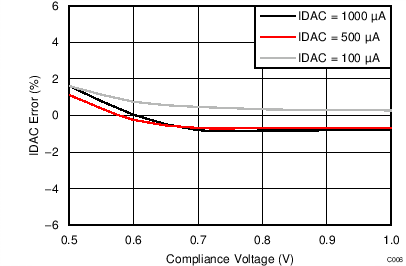
| Compliance voltage | All current settings | AVDD – 0.9 | V | ||||
| Accuracy | All current settings, each IDAC | –6% | ±1% | 6% | |||
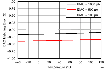
| Current match | Between IDACs | ±0.3% | |||||
| Temperature drift | Each IDAC | 50 | ppm/°C | ||||
| Temperature drift matching | Between IDACs | 10 | ppm/°C | ||||
| TEMPERATURE SENSOR | |||||||
| Conversion resolution | 14 | Bits | |||||
| Temperature resolution | 0.03125 | °C | |||||
| Accuracy | TA = 0°C to +75°C | ±0.25 | °C | ||||
| TA = –40°C to +125°C | ±0.5 | ||||||
| Accuracy vs analog supply voltage | 0.0625 | 0.25 | °C/V | ||||
| LOW-SIDE POWER SWITCH | |||||||
| RON | On-resistance | 3.5 | Ω | ||||
| Current through switch | 30 | mA | |||||
| DIGITAL INPUTS/OUTPUTS | |||||||
| VIH | High-level input voltage | 0.7 DVDD | DVDD | V | |||
| VIL | Low-level input voltage | DGND | 0.3 DVDD | V | |||
| VOH | High-level output voltage | IOH = 3 mA | 0.8 DVDD | V | |||
| VOL | Low-level output voltage | IOL = 3 mA | 0.2 DVDD | V | |||
| IH | Input leakage, high | VIH = 5.5 V | –10 | 10 | µA | ||
| IL | Input leakage, low | VIL = DGND | –10 | 10 | µA | ||
| POWER SUPPLY | |||||||
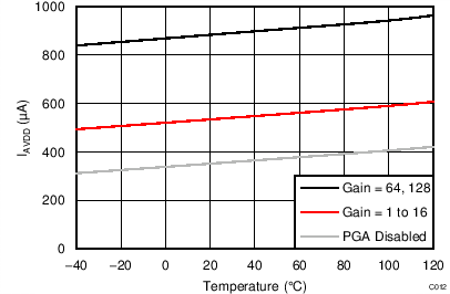
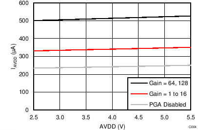
| IAVDD | Analog supply current(3) | Power-down mode | 0.1 | 3 | µA | ||
| Duty-cycle mode, PGA disabled | 65 | ||||||
| Duty-cycle mode, gain = 1 to 16 | 95 | ||||||
| Duty-cycle mode, gain = 32 | 115 | ||||||
| Duty-cycle mode, gain = 64, 128 | 135 | ||||||
| Normal mode, PGA disabled | 240 | ||||||
| Normal mode, gain = 1 to 16 | 340 | 490 | |||||
| Normal mode, gain = 32 | 425 | ||||||
| Normal mode, gain = 64, 128 | 510 | ||||||
| Turbo mode, PGA disabled | 360 | ||||||
| Turbo mode, gain = 1 to 16 | 540 | ||||||
| Turbo mode, gain = 32 | 715 | ||||||
| Turbo mode, gain = 64, 128 | 890 | ||||||
| IDVDD | Digital supply current(3) | Power-down mode | 0.3 | 5 | µA | ||
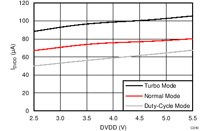
| Duty-cycle mode | 55 | ||||||
| Normal mode | 75 | 110 | |||||
| Turbo mode | 95 | ||||||
| PD | Power dissipation(3) | Duty-cycle mode, PGA disabled | 0.4 | mW | |||
| Normal mode, gain = 1 to 16 | 1.4 | ||||||
| Turbo mode, gain = 1 to 16 | 2.1 | ||||||
(1) PGA disabled means the low-noise PGA is powered down and bypassed. Gains of 1, 2, and 4 are still possible in this case.
See the Bypassing the PGA section for more information.
See the Bypassing the PGA section for more information.
(2) Minimum and maximum values are ensured by design and characterization data.
(3) Internal voltage reference selected, internal oscillator enabled, IDACs turned off, and continuous conversion mode.
Analog supply current increases by 70 µA, typ (normal mode, turbo mode) when selecting an external reference.
Analog supply current increases by 190 µA (typ) when enabling the IDACs (excludes the actual IDAC current).
Analog supply current increases by 70 µA, typ (normal mode, turbo mode) when selecting an external reference.
Analog supply current increases by 190 µA (typ) when enabling the IDACs (excludes the actual IDAC current).
6.6 SPI Timing Requirements
over operating ambient temperature range and DVDD = 2.3 V to 5.5 V (unless otherwise noted)| MIN | MAX | UNIT | |||
|---|---|---|---|---|---|
| td(CSSC) | Delay time, CS falling edge to first SCLK rising edge(2) | 50 | ns | ||
| td(SCCS) | Delay time, final SCLK falling edge to CS rising edge | 25 | ns | ||
| tw(CSH) | Pulse duration, CS high | 50 | ns | ||
| tc(SC) | SCLK period | 150 | ns | ||
| tw(SCH) | Pulse duration, SCLK high | 60 | ns | ||
| tw(SCL) | Pulse duration, SCLK low | 60 | ns | ||
| tsu(DI) | Setup time, DIN valid before SCLK falling edge | 50 | ns | ||
| th(DI) | Hold time, DIN valid after SCLK falling edge | 25 | ns | ||
| SPI timeout(1) | Normal mode, duty-cycle mode | 13955 | t(MOD) | ||
| Turbo mode | 27910 | t(MOD) | |||
(1) See the SPI Timeout section for more information.
t(MOD) = 1 / f(MOD). Modulator frequency f(MOD) = 256 kHz (normal mode, duty-cycle mode) and 512 kHz (turbo mode), when using the internal oscillator or an external 4.096-MHz clock.
t(MOD) = 1 / f(MOD). Modulator frequency f(MOD) = 256 kHz (normal mode, duty-cycle mode) and 512 kHz (turbo mode), when using the internal oscillator or an external 4.096-MHz clock.
(2) CS can be tied low permanently in case the serial bus is not shared with any other device.
6.7 SPI Switching Characteristics
over operating ambient temperature range, DVDD = 2.3 V to 5.5 V (unless otherwise noted)| PARAMETER | TEST CONDITIONS | MIN | TYP | MAX | UNIT | |
|---|---|---|---|---|---|---|
| tp(CSDO) | Propagation delay time, CS falling edge to DOUT driven |
DOUT load = 20 pF || 10 kΩ to DGND | 50 | ns | ||
| tp(SCDO) | Propagation delay time, SCLK rising edge to valid new DOUT |
DOUT load = 20 pF || 10 kΩ to DGND | 0 | 50 | ns | |
| tp(CSDOZ) | Propagation delay time, CS rising edge to DOUT high impedance |
DOUT load = 20 pF || 10 kΩ to DGND | 50 | ns | ||

NOTE: Single-byte communication is shown. Actual communication may be multiple bytes.
Figure 1. Serial Interface Timing Requirements

NOTE:
Single-byte communication is shown. Actual communication may be multiple bytes.6.8 Typical Characteristics
At TA = 25°C, AVDD = 3.3 V, AVSS = 0 V, and PGA enabled using external Vref = 2.5 V (unless otherwise noted).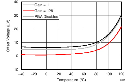
| AVDD = 3.3 V |
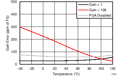
| AVDD = 3.3 V |
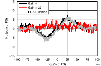
| AVDD = 3.3 V, external 2.5-V reference, normal mode |
Differential Input Signal
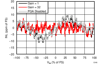
| AVDD = 3.3 V, internal reference, normal mode |
Differential Input Signal
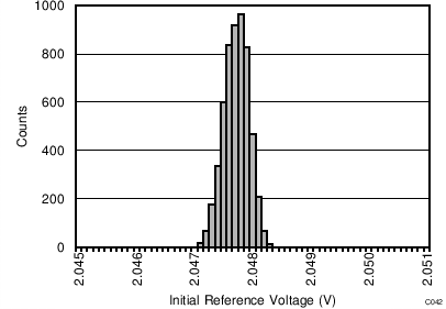
| TA = 25°C, data from 5490 devices |
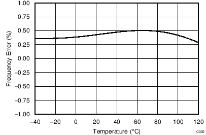
| DVDD = 3.3 V, normal mode |
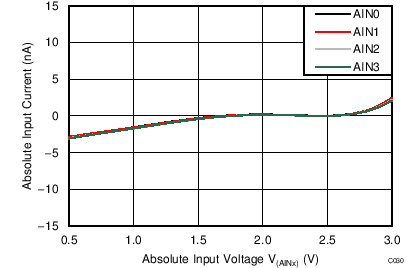
| AVDD = 3.3 V, PGA enabled, TA = –40°C |
Absolute Input Voltage
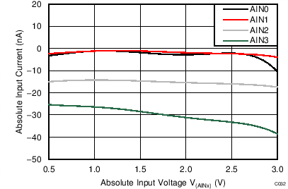
| AVDD = 3.3 V, PGA enabled, TA = 85°C |
Absolute Input Voltage
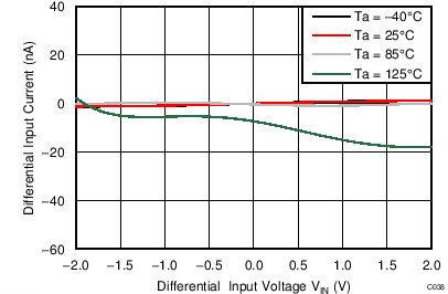
| AVDD = 3.3 V, PGA enabled, AINP = AIN0, AINN = AIN1 |
Differential Input Voltage
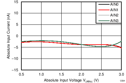
| AVDD = 3.3 V, PGA disabled, TA = –40°C |
Absolute Input Voltage
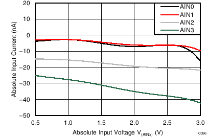
| AVDD = 3.3 V, PGA disabled, TA = 85°C |
Absolute Input Voltage
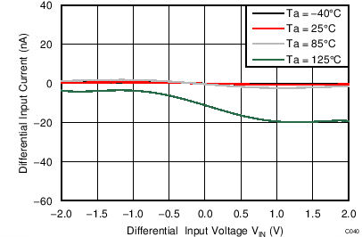
| AVDD = 3.3 V, PGA disabled, AINP = AIN0, AINN = AIN1 |
Differential Input Voltage
| AVDD = 3.3 V, internal reference, turbo mode |
| Normal mode, internal reference |
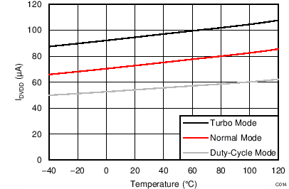
| DVDD = 3.3 V |
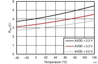
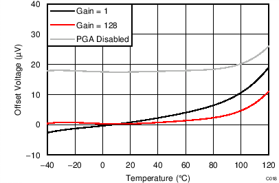
| AVDD = 5.0 V |
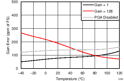
| AVDD = 5.0 V |
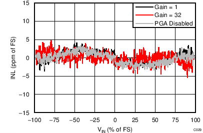
| AVDD = 5.0 V, external 2.5-V reference, normal mode |
Differential Input Signal
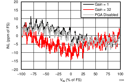
| AVDD = 5.0 V, internal reference, normal mode |
Differential Input Signal
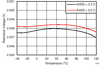
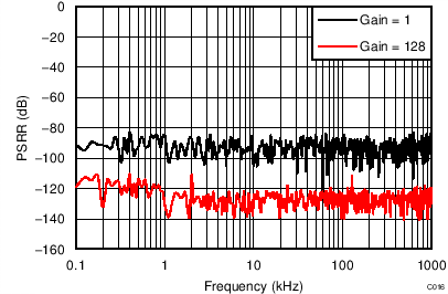
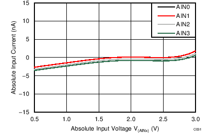
| AVDD = 3.3 V, PGA enabled, TA = 25°C |
Absolute Input Voltage
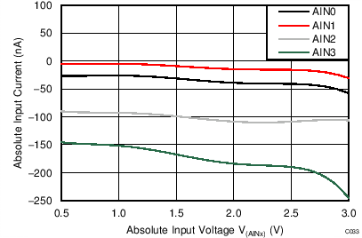
| AVDD = 3.3 V, PGA enabled, TA = 125°C |
Absolute Input Voltage
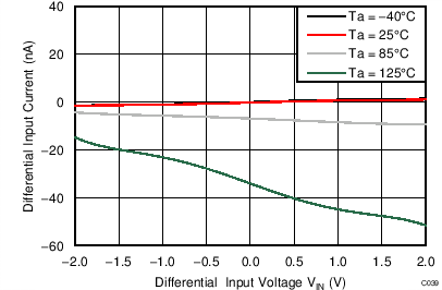
| AVDD = 3.3 V, PGA enabled, AINP = AIN3, AINN = AIN2 |
Differential Input Voltage
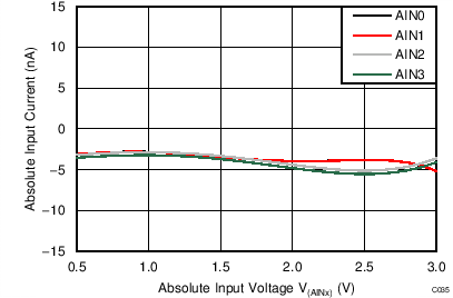
| AVDD = 3.3 V, PGA disabled, TA = 25°C |
Absolute Input Voltage
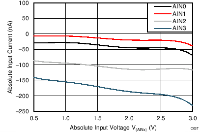
| AVDD = 3.3 V, PGA disabled, TA = 125°C |
Absolute Input Voltage
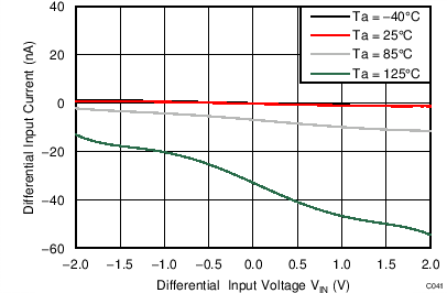
| AVDD = 3.3 V, PGA disabled, AINP = AIN3, AINN = AIN2 |
Differential Input Voltage
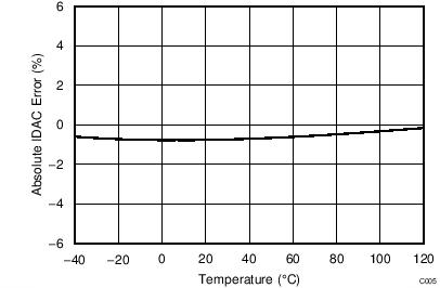
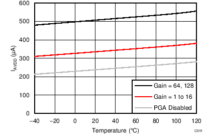
| AVDD = 3.3 V, internal reference, normal mode |
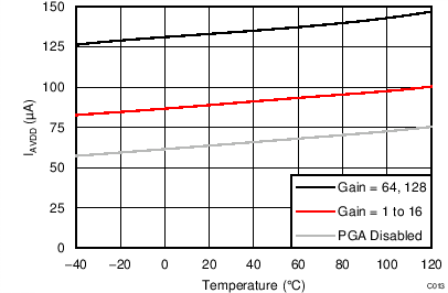
| AVDD = 3.3 V, internal reference, duty-cycle mode |
