-
TPD3S0x4 针对 USB 主机端口的限流开关和 D+/D– ESD 保护
- 1 特性
- 2 应用
- 3 说明
- 4 简化电路原理图
- 5 修订历史记录
- 6 Device Comparison
- 7 Pin Configuration and Functions
- 8 Specifications
- 9 Detailed Description
- 10Application and Implementation
- 11Power Supply Recommendations
- 12Layout
- 13器件和文档支持
- 14机械封装和可订购信息
- 重要声明
DATA SHEET
TPD3S0x4 针对 USB 主机端口的限流开关和 D+/D– ESD 保护
本资源的原文使用英文撰写。 为方便起见,TI 提供了译文;由于翻译过程中可能使用了自动化工具,TI 不保证译文的准确性。 为确认准确性,请务必访问 ti.com 参考最新的英文版本(控制文档)。
1 特性
2 应用
- USB 端口/集线器
- 便携式计算机,台式机
- 高清数字电视
- 机顶盒
3 说明
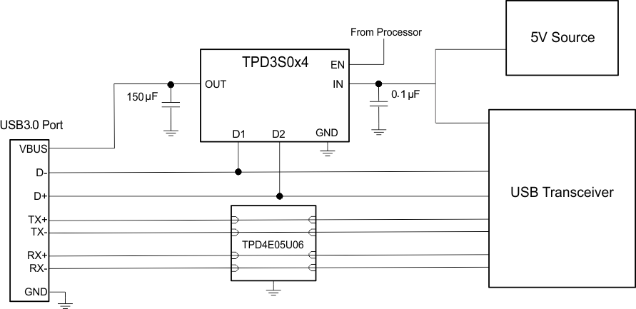
TPD3S0x4 集成器件配有一个限流负载开关和一个基于双通道瞬态电压抑制器 (TVS) 的静电放电 (ESD) 保护二极管阵列,适用于 USB 接口。
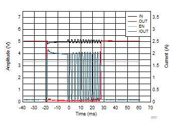
TPD3S0x4 器件适用于可能出现大电容负载和短路的应用(如 USB 接口);TPD3S0x4 可提供短路保护和过流保护。 当输出负载超过电流限制阈值时,TPD3S0x4 通过在恒定电流模式下运行即可将输出电流限制到安全水平。 快速过载响应特性有助于减轻 5V 主电源的负担,当输出短路时可以快速调节电源。 电流限制开关的上升和下降此时受到控制,力求尽量减小器件开关过程中的浪涌电流。
TPD3S014 和 TPD3S044 的连续电流分别为 0.5A 和 1.5A。 TVS 二极管阵列的额定 ESD 冲击消散值高于 IEC 61000-4-2 国际标准中规定的最高水平。 此器件高度集成,并且采用易于布线的 DBV 封装,可对便携式计算机、高清数字 TV 和机顶盒等应用中的 USB 接口提供强力的电路保护。
器件信息(1)
| 器件型号 | 封装 | 封装尺寸(标称值) |
|---|---|---|
| TPD3S0x4 | DBV (6) | 2.90mm x 2.80mm |
- 要了解所有可用封装,请见数据表末尾的可订购产品附录。
4 简化电路原理图
6 Device Comparison
| PART NUMBER | MAXIMUM OPERATING CURRENT | OUTPUT DISCHARGE | ENABLE | PACKAGED DEVICE AND MARKING SOT23-6 (DBV) |
|---|---|---|---|---|
| TPD3S014 | 0.5 A | Y | High | SII |
| TPD3S044 | 1.5 A | Y | High | SIJ |
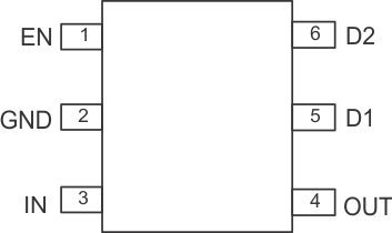
7 Pin Configuration and Functions
DBV PACKAGE
SOT23 6-PIN
(2.9 mm × 2.8 mm × 1.45 mm)
Pin Functions
| PIN | DESCRIPTION | |
|---|---|---|
| NAME | NO. | |
| D1 | 5 | USB data+ or USB data– |
| D2 | 6 | |
| EN | 1 | Enable input, logic high turns on power switch |
| GND | 2 | Ground |
| IN | 3 | Input voltage and power-switch drain; Connect a 0.1 µF or greater ceramic capacitor from IN to GND close to the IC |
| OUT | 4 | Power-switch output, connect to load |
8 Specifications
8.1 Absolute Maximum Ratings
over operating free-air temperature (unless otherwise noted)(1)(2)| MIN | MAX | UNIT | ||
|---|---|---|---|---|
| Input voltage(3) | VIN | –0.3 | 6 | V |
| VOUT | –0.3 | 6 | ||
| EN | –0.3 | 6 | ||
| D1 | –0.3 | 6 | ||
| D2 | –0.3 | 6 | ||
| Voltage range from VIN to VOUT | –6 | 6 | V | |
| Junction temperature, TJ | Internally limited | |||
| Storage temperature range, Tstg | –65 | 150 | °C | |
(1) Stresses beyond those listed under Absolute Maximum Ratings may cause permanent damage to the device. These are stress ratings only, which do not imply functional operation of the device at these or any other conditions beyond those indicated under Recommended Operating Conditions. Exposure to absolute-maximum-rated conditions for extended periods may affect device reliability.
(2) Voltages are with respect to GND unless otherwise noted.
(3) See the Input and Output Capacitance section.
8.2 ESD Ratings
| VALUE | UNIT | |||||
|---|---|---|---|---|---|---|
| V(ESD) | Electrostatic discharge | Human body model (HBM), per ANSI/ESDA/JEDEC JS-001(1) | All pins | ±2000 | V | |
| Charged device model (CDM), per JEDEC specification JESD22-C101(2) | All pins | ±500 | ||||
| IEC 61000-4-2 Contact Discharge(3) | VOUT, Dx pins | ±12000 | ||||
| IEC 61000-4-2 Air-Gap Discharge(3) | VOUT, Dx pins | ±15000 | ||||
(1) JEDEC document JEP155 states that 500-V HBM allows safe manufacturing with a standard ESD control process. Pins listed as ±2000 V may actually have higher performance.
(2) JEDEC document JEP157 states that 250-V CDM allows safe manufacturing with a standard ESD control process. Pins listed as ±500 V may actually have higher performance.
(3) VOUT was tested on a PCB with input and output bypassing capacitors of 0.1 µF and 120 µF, respectively.
8.3 Recommended Operating Conditions
over operating free-air temperature range (unless otherwise noted)| MIN | NOM | MAX | UNIT | ||
|---|---|---|---|---|---|
| VIN | Input voltage | 4.5 | 5.5 | V | |
| VEN | Input voltage, EN | 0 | 5.5 | V | |
| VIH | High-level Input voltage, EN | 2 | V | ||
| VIL | Low-level Input voltage, EN | 0.7 | V | ||
| CIN | Input de-coupling capacitance, IN to GND | 0.1 | µF | ||
| IOUT(1) | Continuous output current (TPD3S014) | 0.5 | A | ||
| Continuous output current (TPD3S044) | 1.5 | ||||
| TJ | Operating junction temperature | –40 | 125 | °C | |
(1) Package and current ratings may require an ambient temperature derating of 85°C
8.4 Thermal Information
| THERMAL METRIC(1)(2) | TPD3S0x4 | UNIT | |
|---|---|---|---|
| DBV | |||
| 6 PINS | |||
| RθJA | Junction-to-ambient thermal resistance | 185.8 | °C/W |
| RθJC(top) | Junction-to-case (top) thermal resistance | 124.7 | |
| RθJB | Junction-to-board thermal resistance | 32.0 | |
| ψJT | Junction-to-top characterization parameter | 23.7 | |
| ψJB | Junction-to-board characterization parameter | 31.5 | |
| RθJC(bot) | Junction-to-case (bottom) thermal resistance | N/A | |
| RθJA(Custom) | See the Power Dissipation and Junction Temperature section | 120.3 | |
(1) For more information about traditional and new thermal metrics, see the IC Package Thermal Metrics application report, SPRA953.
(2) See Device Comparison Table.
8.5 Electrical Characteristics: TJ = TA = 25°C
Unless otherwise noted: VIN = 5 V, VEN = VIN, IOUT = 0 A. See Device Comparison for the rated current of each part number. Parametrics over a wider operational range are shown in the second Electrical Characteristics: –40°C ≤ TJ ≤ 125°C table.| PARAMETER | TEST CONDITIONS(1) | MIN | TYP | MAX | UNIT | |
|---|---|---|---|---|---|---|
| POWER SWITCH | ||||||
| RDS(on) | Input – Output resistance | TPD3S014 | 97 | 110 | mΩ | |
| TPD3S014: –40°C ≤ (TJ, TA) ≤ 85°C | 96 | 130 | ||||
| TPD3S044 | 74 | 91 | ||||
| TPD3S044: –40°C ≤ (TJ, TA) ≤ 85°C | 74 | 106 | ||||
| CURRENT LIMIT | ||||||
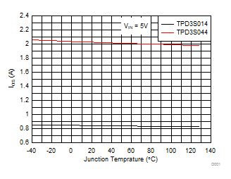
| IOS(2) | Current limit, see Figure 27 | TPD3S014 | 0.67 | 0.85 | 1.01 | A |
| TPD3S044 | 1.70 | 2.15 | 2.50 | |||
| SUPPLY CURRENT | ||||||
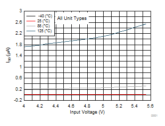
| ISD | Supply current, switch disabled | IOUT = 0A | 0.02 | 1 | µA | |
| –40°C ≤ (TJ, TA) ≤ 85°C, VIN = 5.5 V, IOUT = 0 A | 2 | |||||
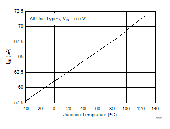
| ISE | Supply current, switch enabled | IOUT = 0A | 66 | 74 | µA | |
| –40°C ≤ (TJ, TA) ≤ 85°C, VIN = 5.5 V, IOUT = 0 A | 85 | |||||
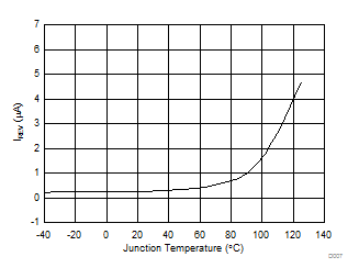
| IREV | Reverse leakage current | VOUT = 5 V, VIN = 0 V, Measure IVOUT | 0.2 | 1 | µA | |
| –40°C ≤ (TJ, TA) ≤ 85°C, VOUT = 5 V, VIN = 0 V, measure IVOUT | 5 | |||||
| OUTPUT DISCHARGE | ||||||
| RPD | Output pull-down resistance(3) | VIN = VOUT = 5 V, disabled | 400 | 456 | 600 | Ω |
| ESD PROTECTION | ||||||
| ΔCIO | Differential capacitance between the D1, D2 lines | ƒ = 1 MHz, VIO = 2.5 V | 0.02 | pF | ||
| CIO | (D1, D2 to GND) | ƒ = 1 MHz, VIO = 2.5 V | 1.4 | pF | ||
| RDYN | Dynamic on-resistance D1, D2 IEC clamps(4) | Dx to GND | 0.2 | Ω | ||
| GND to Dx | ||||||
(1) Pulsed testing techniques maintain junction temperature approximately equal to ambient temperature
(2) See Current Limit for explanation of this parameter.
(3) These Parameters are provided for reference only, and do not constitute a part of TI’s published device specifications for purposes of TI’s product warranty.
(4) RDYN was extracted using the least squares first of the TLP characteristics between I = 20A and I = 30A.
8.6 Electrical Characteristics: –40°C ≤ TJ ≤ 125°C
Unless otherwise noted: 4.5 V ≤ VIN ≤ 5.5 V, VEN = VIN, IOUT = 0 A, typical values are at 5 V and 25°C. See the Device Comparison for the rated current of each part number.| PARAMETER | TEST CONDITIONS(1) | MIN | TYP | MAX | UNIT | |
|---|---|---|---|---|---|---|
| POWER SWITCH | ||||||
| RDS(on) | Input – output resistance | TPD3S014 | 97 | 154 | mΩ | |
| TPD3S044 | 74 | 121 | ||||
| ENABLE INPUT (EN) | ||||||
| Threshold | Input rising | 1 | 1.45 | 2 | V | |
| Hysteresis | 0.13 | V | ||||
| Leakage current | VEN = 0 V | –1 | 0 | 1 | µA | |
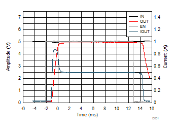
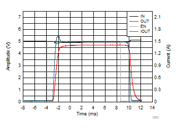
| tON | Turn on time | VIN = 5 V, CL = 1 µF, RL = 100 Ω, EN ↑ See Figure 26 |
1 | 1.6 | 2.2 | ms |
| tOFF | Turn off time | VIN = 5 V, CL = 1 µF, RL = 100 Ω, EN ↓ See Figure 26 |
1.7 | 2.1 | 2.7 | ms |
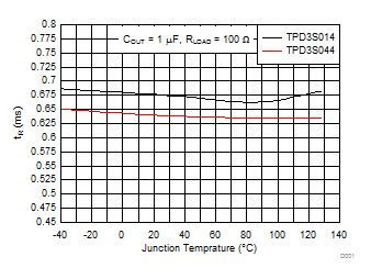
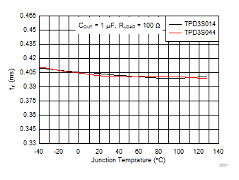
| tR | Rise time, output | CL = 1 µF, RL = 100 Ω, VIN = 5 V, See Figure 25 | 0.4 | 0.64 | 0.9 | ms |
| tF | Fall time, output | CL = 1 µF, RL = 100 Ω, VIN = 5 V, See Figure 25 | 0.25 | 0.4 | 0.8 | ms |
| CURRENT LIMIT | ||||||
| IOS(2) | Current limit, see Figure 27 | TPD3S014 | 0.65 | 0.85 | 1.05 | A |
| TPD3S044 | 1.60 | 2.15 | 2.70 | |||
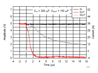
| tIOS | Short-circuit response time(3) | VIN = 5 V (see Figure 27) One Half full load → RSHORT = 50 mΩ Measure from application to when current falls below 120% of final value |
2 | µs | ||
| SUPPLY CURRENT | ||||||
| ISD | Supply current, switch disabled | IOUT = 0 A | 0.02 | 10 | µA | |
| ISE | Supply current, switch enabled | IOUT = 0 A | 66 | 94 | µA | |
| IREV | Reverse leakage current | VOUT = 5.5 V, VIN = 0 V, Measure IVOUT | 0.2 | 20 | µA | |
| UNDERVOLTAGE LOCKOUT | ||||||
| VUVLO | Rising threshold | VIN↑ | 3.5 | 3.77 | 4 | V |
| Hysteresis | VIN↓ | 0.14 | V | |||
| OUTPUT DISCHARGE | ||||||
| RPD | Output pull-down resistance | VIN = 4 V, VOUT = 5 V, Disabled | 350 | 545 | 1200 | Ω |
| VIN = 5 V, VOUT = 5 V, Disabled | 300 | 456 | 800 | |||
| THERMAL SHUTDOWN | ||||||
| TSHDN | Rising threshold (TJ) | In current limit | 135 | °C | ||
| Not in current limit | 155 | |||||
| Hysteresis(3) | 20 | °C | ||||
| ESD PROTECTION | ||||||
| II | Input leakage current (D1, D2) | VI = 3.3 V | 0.02 | 1 | µA | |
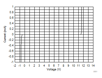
| VD | Diode forward voltage (D1, D2); Lower clamp diode | IO = 8 mA | 0.95 | V | ||
| VBR | Breakdown voltage (D1, D2) | IBR = 1 mA | 6 | V | ||
(1) Pulsed testing techniques maintain junction temperature approximately equal to ambient temperature
(2) See Current Limit section for explanation of this parameter.
(3) These parameters are provided for reference only, and do not constitute part of TI’s published device specifications for purposes of TI’s product warranty.
8.7 Typical Characteristics
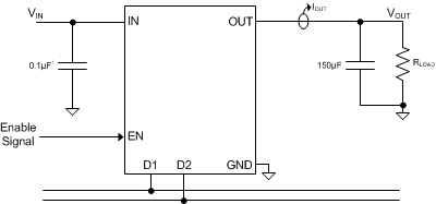
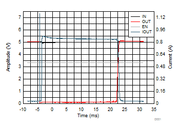
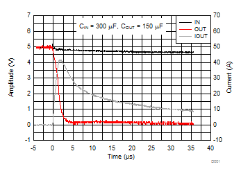
1. During the short applied tests, 300µF is used because of the use of an external supply.
Figure 1. Test Circuit for System Operation in Typical Characteristics
