DATA SHEET
TPS7A8101 低噪声、高带宽、高 PSRR、低压降 1A 线性稳压器
本资源的原文使用英文撰写。 为方便起见,TI 提供了译文;由于翻译过程中可能使用了自动化工具,TI 不保证译文的准确性。 为确认准确性,请务必访问 ti.com 参考最新的英文版本(控制文档)。
1 特性
2 应用范围
- 电信基础设施
- 音频
- 高速接口 (I/F)(锁相环 (PLL) 和压控振荡器 (VCO))
3 说明
TPS7A8101是一款低压差线性稳压器(LDO),此稳压器可在噪音情况下可提供出色的性能以及输出端的电源抑制比(PSRR)。这个LDO使用一个先进的双极CMOS(BiCMOS)工艺和一个功率场效应晶体管(PMOSFET)无源器件来实现极低噪音,优良的瞬态响应,和出色的PSRR性能。
TPS7A8101 器件与 4.7μF 陶瓷输出电容搭配工作时可保持稳定,并且使用了一个精密电压基准和反馈环路,从而在所有负载、线路、过程和温度变化范围内至少实现 3% 的精度。
该器件的额定温度范围为 TJ = –40°C 至 125°C,采用带有散热焊盘的 3mm × 3mm、小外形尺寸无引线 (SON)-8 封装。
器件信息(1)
| 器件型号 | 封装 | 封装尺寸(标称值) |
|---|---|---|
| TPS7A8101 | SON (8) | 3.00mm x 3.00mm |
- 要了解所有可用封装,请见数据表末尾的可订购产品附录。
典型应用电路

5 Pin Configuration and Functions
DRB PACKAGE
8-Pin SON With Exposed Thermal Pad
Top View

Pin Functions
| PIN | I/O | DESCRIPTION | |
|---|---|---|---|
| NAME | NO. | ||
| EN | 5 | I | Driving this pin high turns on the regulator. Driving this pin low puts the regulator into shutdown mode. Refer to the Shutdown section for more details. EN must not be left floating and can be connected to IN if not used. |
| FB | 3 | I | This pin is the input to the control-loop error amplifier and is used to set the output voltage of the device. |
| GND | 4, pad | — | Ground |
| IN | 7 | I | Unregulated input supply |
| 8 | |||
| NR | 6 | — | Connect an external capacitor between this pin and ground to reduce output noise to very low levels. The capacitor also slows down the VOUT ramp (RC softstart). |
| OUT | 1 | O | Regulator output. A 4.7-μF or larger capacitor of any type is required for stability. |
| 2 | |||
6 Specifications
6.1 Absolute Maximum Ratings
Over operating free-air temperature range (unless otherwise noted).(1)| MIN | MAX | UNIT | ||
|---|---|---|---|---|
| Voltage | IN | –0.3 | 7 | V |
| FB, NR | –0.3 | 3.6 | ||
| EN | –0.3 | VIN + 0.3(2) | ||
| OUT | –0.3 | 7 | ||
| Current | OUT | Internally Limited | A | |
| Temperature | Operating virtual junction, TJ | –55 | 150 | °C |
| Storage, Tstg | –55 | 150 | °C | |
(1) Stresses beyond those listed under Absolute Maximum Ratings may cause permanent damage to the device. These are stress ratings only, and functional operation of the device at these or any other conditions beyond those indicated is not implied. Exposure to absolute-maximum-rated conditions for extended periods my affect device reliability.
(2) VEN absolute maximum rating is VIN + 0.3 V or +7 V, whichever is smaller.
6.2 ESD Ratings
| VALUE | UNIT | ||||
|---|---|---|---|---|---|
| V(ESD) | Electrostatic discharge | Human body model (HBM), per ANSI/ESDA/JEDEC JS-001, all pins(1) | ±2000 | V | |
| Charged device model (CDM), per JEDEC specification JESD22-C101, all pins(2) | ±500 | ||||
(1) JEDEC document JEP155 states that 500-V HBM allows safe manufacturing with a standard ESD control process.
(2) JEDEC document JEP157 states that 250-V CDM allows safe manufacturing with a standard ESD control process.
6.3 Recommended Operating Conditions
Over operating free-air temperature range (unless otherwise noted)| MIN | MAX | UNIT | ||
|---|---|---|---|---|
| VI | Input voltage | 2.2 | 6.5 | V |
| IO | Output current | 0 | 1 | A |
| TA | Operating free air temperature | –40 | 125 | °C |
6.4 Thermal Information
| THERMAL METRIC(1) | TPS7A8101 | UNIT | |
|---|---|---|---|
| DRV (SON) | |||
| 8 PINS | |||
| RθJA | Junction-to-ambient thermal resistance | 47.8 | °C/W |
| RθJC(top) | Junction-to-case (top) thermal resistance | 53.9 | °C/W |
| RθJB | Junction-to-board thermal resistance | 23.4 | °C/W |
| ψJT | Junction-to-top characterization parameter | 1 | °C/W |
| ψJB | Junction-to-board characterization parameter | 23.5 | °C/W |
| RθJC(bot) | Junction-to-case (bottom) thermal resistance | 7.4 | °C/W |
(1) For more information about traditional and new thermal metrics, see the Semiconductor and IC Package Thermal Metrics application report, SPRA953.
6.5 Electrical Characteristics
Over the operating temperature range of TJ = –40°C to +125°C, VIN = VOUT(TYP) + 0.5 V or 2.2 V (whichever is greater), IOUT = 1 mA, VEN = 2.2 V, COUT = 4.7 μF, CNR = 0.01 μF, and CBYPASS = 0 μF, unless otherwise noted. TPS7A8101 is tested at VOUT = 0.8 V and VOUT = 6 V. Typical values are at TJ = 25°C.| PARAMETER | TEST CONDITIONS | MIN | TYP | MAX | UNIT | |||
|---|---|---|---|---|---|---|---|---|
| VIN | Input voltage range(1) | 2.2 | 6.5 | V | ||||
| VNR | Internal reference | 0.79 | 0.8 | 0.81 | V | |||
| VOUT | Output voltage range | 0.8 | 6 | V | ||||
| Output accuracy(2) | VOUT + 0.5 V ≤ VIN ≤ 6 V, VIN ≥ 2.5 V, 100 mA ≤ IOUT ≤ 500 mA, 0°C ≤ TJ ≤ 85°C |
-2% | 2% | |||||
| VOUT + 0.5 V ≤ VIN ≤ 6.5 V, VIN ≥ 2.2 V, 100 mA ≤ IOUT ≤ 1 A |
–3% | ±0.3% | 3% | |||||
| ΔVO(ΔVI) | Line regulation | VOUT(NOM) + 0.5 V ≤ VIN ≤ 6.5 V, VIN ≥ 2.2 V, IOUT = 100 mA |
150 | μV/V | ||||
| ΔVO(ΔIL) | Load regulation | 100 mA ≤ IOUT ≤ 1 A | 2 | μV/mA | ||||
| VDO | Dropout voltage(3) | VOUT + 0.5 V ≤ VIN ≤ 6.5 V, VIN ≥ 2.2 V, IOUT = 500 mA, VFB = GND or VSNS = GND |
250 | mV | ||||
| VOUT + 0.5 V ≤ VIN ≤ 6.5 V, VIN ≥ 2.5 V, IOUT = 750 mA, VFB = GND or VSNS = GND |
350 | |||||||
| VOUT + 0.5 V ≤ VIN ≤ 6.5 V, VIN ≥ 2.5 V, IOUT = 1 A, VFB = GND or VSNS = GND |
500 | |||||||
| ILIM | Output current limit | VOUT = 0.85 × VOUT(NOM), VIN ≥ 3.3 V | 1100 | 1400 | 2000 | mA | ||
| IGND | Ground pin current | IOUT = 1 mA | 60 | 100 | μA | |||
| IOUT = 1 A | 350 | |||||||
| ISHDN | Shutdown current (IGND) | VEN ≤ 0.4 V, VIN ≥ 2.2 V, RL = 1 kΩ, 0°C ≤ TJ ≤ 85°C |
0.2 | 2 | μA | |||
| IFB | Feedback pin current | VIN = 6.5 V, VFB = 0.8 V | 0.02 | 1 | μA | |||
| PSRR | Power-supply rejection ratio | VIN = 4.3 V, VOUT = 3.3 V, IOUT = 750 mA |
f = 100 Hz | 80 | dB | |||
| f = 1 kHz | 82 | |||||||
| f = 10 kHz | 78 | |||||||
| f = 100 kHz | 60 | |||||||
| f = 1 MHz | 54 | |||||||
| Vn | Output noise voltage | BW = 100 Hz to 100 kHz, VIN = 3.8 V, VOUT = 3.3 V, IOUT = 100 mA, CNR = CBYPASS = 470 nF |
23.5 | μVRMS | ||||
| VEN(HI) | Enable high (enabled) | 2.2 V ≤ VIN ≤ 3.6 V, RL = 1 kΩ | 1.2 | V | ||||
| 3.6 V < VIN ≤ 6.5 V, RL = 1 kΩ | 1.35 | |||||||
| VEN(LO) | Enable low (shutdown) | RL = 1 kΩ | 0 | 0.4 | V | |||
| IEN(HI) | Enable pin current, enabled | VIN = VEN = 6.5 V | 0.02 | 1 | μA | |||
| tSTR | Start-up time | VOUT(NOM) = 3.3 V, VOUT = 0% to 90% VOUT(NOM), RL = 3.3 kΩ, COUT = 10 μF, CNR = 470 nF |
80 | ms | ||||
| UVLO | Undervoltage lockout | VIN rising, RL = 1 kΩ | 1.86 | 2 | 2.10 | V | ||
| Hysteresis | VIN falling, RL = 1 kΩ | 75 | mV | |||||
| TSD | Thermal shutdown temperature | Shutdown, temperature increasing | 160 | °C | ||||
| Reset, temperature decreasing | 140 | °C | ||||||
| TJ | Operating junction temperature | –40 | 125 | °C | ||||
(1) Minimum VIN = VOUT + VDO or 2.2 V, whichever is greater.
(2) The TPS7A8101 does not include external resistor tolerances and it is not tested at this condition: VOUT = 0.8 V, 4.5V ≤ VIN ≤ 6.5 V, and 750 mA ≤ IOUT ≤ 1 A because the power dissipation is greater than the maximum rating of the package.
(3) VDO is not measured for fixed output voltage devices with VOUT < 1.7 V because minimum VIN = 2.2 V.
6.6 Typical Characteristics
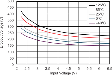
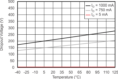
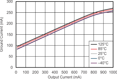
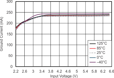
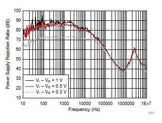
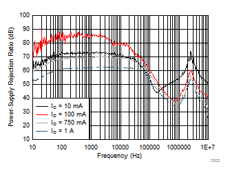
At VOnom = 3.3 V, VI = VOnom + 0.5 V or 2.2 V (whichever is greater), IO = 100 mA, V(EN) = VI, C(IN) = 1 μF, C(OUT) = 4.7 μF, and C(NR) = 0.01 μF; all temperature values refer to TJ, unless otherwise noted.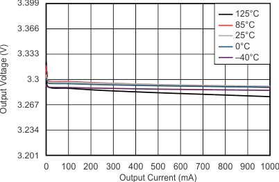
| NOTE: The Y-axis shows 1% VO per division | ||

| VO = 0.8 V | IO = 750 mA | |
| NOTE: The Y-axis shows 1% VO per division | ||
| IO = 1 A | ||

| IO = 500 mA | ||
| VI = 3.6 V | ||
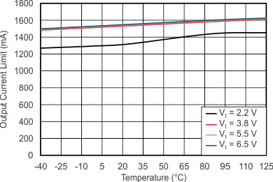
| VO = VI – 0.5 V |
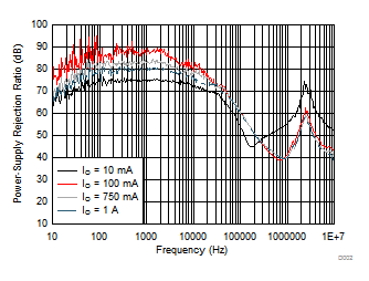
| VI – VO = 1 V | C(IN) = 0 F | C(OUT) = 10 µF |
| C(NR) = C(BYPASS) = 470 nF | ||
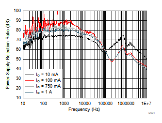
| VI – VO = 1 V | C(IN) = 0 F | C(OUT) = 10 µF |
| C(NR) = C(BYPASS) = 470 nF | ||
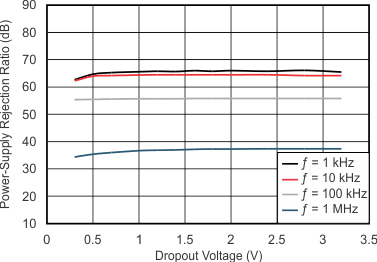
| IO = 100 mA | C(IN) = 0 F |

| VI – VO = 0.5 V | C(OUT) = 10 µF | C(IN) = 10 µF | |
| 24.09 µVRMS (C(NR) = C(BYPASS) = 100 nF) | |||
| 23.54 µVRMS (C(NR) = C(BYPASS) = 470 nF) | |||
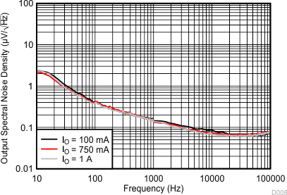
| 23.54 µVRMS (IO = 100 mA) | C(IN) = 10 µF | VI – VO = 0.5 V |
| 23.71 µVRMS (IO = 750 mA) | C(NR) = 470 nF | C(OUT) = 10 µF |
| 22.78 µVRMS (IO = 1 A) | C(BYPASS) = 470 nF | |

| Using the same value of C(NR) and C(BYPASS) in the X-Axis |
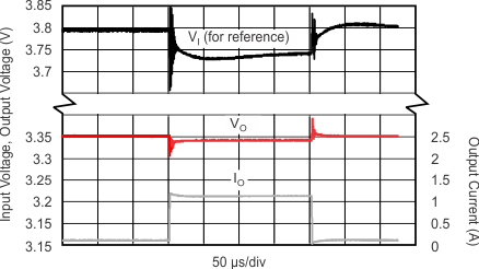
| IO = 100 mA → 1 A → 100 mA | ||
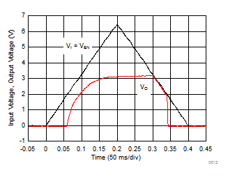
| RL = 33 Ω | C(NR) = 470 nF | C(BYPASS) = 470 nF | ||
| C(OUT) = 10 µF | C(IN) = 10 µF | |||
| (1) The internal reference requires approximately 80 ms of rampup time (see Start-Up) from the enable event; therefore, VO fully reaches the target output voltage of 3.3 V in 80 ms from start-up. | ||||

| NOTE: The Y-axis shows 1% VO per division | ||

| VO = 0.8 V | IO = 5 mA | |
| NOTE: The Y-axis shows 1% VO per division | ||
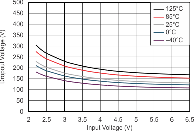
| IO = 750 mA | ||

| VI = 3.6 V | ||
| VO = 0.8 V | IO = 750 mA | |
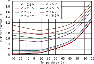
| V(EN) = 0.4 V | ||
| C(NR) = C(BYPASS) = 470 nF | C(OUT) = 10 µF | C(IN) = 0 F |
| VI – VO = 0.5 V | C(IN) = 0 F | C(OUT) = 10 µF |
| C(NR) = C(BYPASS) = 470 nF | ||
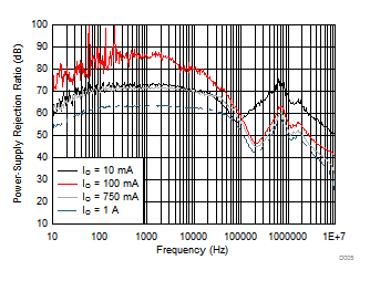
| VI – VO = 0.5 V | C(IN) = 0 F | C(OUT) = 10 µF |
| C(NR) = C(BYPASS) = 470 nF | ||

| IO = 750 mA | C(IN) = 0 F |
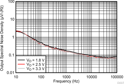
| 25.89 µVRMS (VO = 1.8 V) | C(IN) = 10 µF | VI – VO = 0.5 V |
| 23.54 µVRMS (VO = 2.5 V) | C(NR) = 470 nF | C(OUT) = 10 µF |
| 23.54 µVRMS (VO = 3.3 V) | C(BYPASS) = 470 nF | |
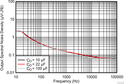
| 23.54 µVRMS (CO = 10 µF) | C(IN) = 10 µF | VI – VO = 0.5 V |
| 23.91 µVRMS (CO = 22 µF) | C(NR) = 470 nF | C(OUT) = 10 µF |
| 22.78 µVRMS (CO = 100 µF) | C(BYPASS) = 470 nF | |
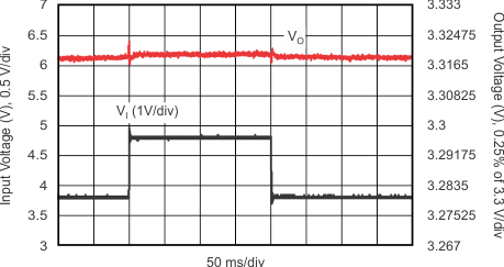
| VI = 3.8 V → 4.8 V → 3.8 V | ||
| IO = 500 mA | ||
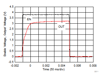
| RL = 33 Ω | C(NR) = 470 nF | C(BYPASS) = 470 nF |
| C(OUT) = 10 µF | C(IN) = 10 µF |