-
ADS85x8 12 位、14 位和 16 位 8 通道同时采样 ADC
- 1 特性
- 2 应用
- 3 说明
- 4 修订历史记录
- 5 Device Comparison Table
- 6 Pin Configuration and Functions
-
7 Specifications
- 7.1 Absolute Maximum Ratings
- 7.2 ESD Ratings
- 7.3 Recommended Operating Conditions
- 7.4 Thermal Information
- 7.5 Electrical Characteristics: General
- 7.6 Electrical Characteristics: ADS8528
- 7.7 Electrical Characteristics: ADS8548
- 7.8 Electrical Characteristics: ADS8568
- 7.9 Serial Interface Timing Requirements
- 7.10 Parallel Interface Timing Requirements (Read Access)
- 7.11 Parallel Interface Timing Requirements (Write Access)
- 7.12 Typical Characteristics
- 8 Parameter Measurement information
- 9 Detailed Description
- 10Application and Implementation
- 11Power Supply Recommendations
- 12Layout
- 13器件和文档支持
- 14机械、封装和可订购信息
- 重要声明
DATA SHEET
ADS85x8 12 位、14 位和 16 位 8 通道同时采样 ADC
本资源的原文使用英文撰写。 为方便起见,TI 提供了译文;由于翻译过程中可能使用了自动化工具,TI 不保证译文的准确性。 为确认准确性,请务必访问 ti.com 参考最新的英文版本(控制文档)。
1 特性
- 12 位、14 位和 16 位 ADC 系列(各成员器件的引脚和软件彼此兼容)
- 每通道的最大数据速率:
- ADS8528:650kSPS (PAR) 或
480kSPS (SER) - ADS8548:600kSPS (PAR) 或
450kSPS (SER) - ADS8568:510kSPS (PAR) 或
400kSPS (SER)
- ADS8528:650kSPS (PAR) 或
- 出色的交流性能:
- 信噪比:
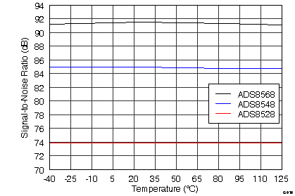
ADS8528:73.9dB;ADS8548:85dB;ADS8568:91.5dB - 总谐波失真:
ADS8528:–89dB;ADS8548:–91dB;ADS8568:–94dB
- 信噪比:
- 可编程、经缓冲的内部基准:
0.5V–2.5V 或 0.5V–3.0V,最高支持 ±12V 的输入电压范围 - 可选并行或串行接口
- 采用自动休眠模式的可扩展低功耗操作:10kSPS 时仅为 32mW
- 可在扩展工业温度范围内完全额定运行
2 应用
- 保护中继器
- 电源质量测量
- 多轴电机控制
- 可编程逻辑控制器
- 工业数据采集
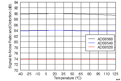
SNR 与温度间的关系
3 说明
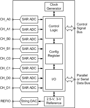
ADS85x8 具备 8 个基于逐次逼近寄存器 (SAR) 的低功耗 12 位、14 位或 16 位模数转换器 (ADC),每个 ADC 都配有真正的双极输入。这些通道分组为四对,能够以高达 650kSPS 的速率同时采集信号。
这些器件允许选择并行或串行接口,并且支持菊花链连接。可编程基准允许处理幅值最高可达 ±12V 的模拟输入信号。
ADS85x8 系列采用 64 引脚超薄四方扁平无引线 (VQFN) 和薄型四方扁平 (LQFP) 封装,并且支持自动休眠模式,可最大限度地降低功耗。整个系列的额定工作温度范围为 -40℃ 至 +125℃。
器件信息(1)
| 器件型号 | 封装 | 封装尺寸(标称值) |
|---|---|---|
| ADS85x8 | VQFN (64) | 9.00mm x 9.00mm |
| LQFP (64) | 10.00mm x 10.00mm |
- 要了解所有可用封装,请参见数据表末尾的可订购产品附录。
简化框图
4 修订历史记录
Changes from B Revision (November 2015) to C Revision
Changes from A Revision (October 2011) to B Revision
- 已添加 ESD 额定值表,建议运行条件表,特性 描述部分,器件功能模式部分,寄存器映射部分,应用和实施部分,电源相关建议部分,布局部分,器件和文档支持部分以及机械、封装和可订购信息部分Go
- Changed title of Device Comparison Table, deleted footnote 1 Go
- Added Storage temperature parameter to Absolute Maximum Ratings tableGo
- Changed Clock cycles per conversion to be a single parameter instead of part of tCONV parameter in Serial Interface Timing Requirements table Go
- Changed tBUFS parameter in Serial Interface Timing Requirements tableGo
- Added footnote 3 to Serial Interface Timing Requirements tableGo
- Changed Clock cycles per conversion to be a single parameter instead of part of tCONV parameter in Parallel Interface Timing Requirements (Read Access) table Go
- Changed tBUCS parameter in Parallel Interface Timing Requirements (Read Access) table Go
- Added footnote 3 to Parallel Interface Timing Requirements (Read Access) table Go
- Changed Data Readout and BUSY/INT Signal sectionGo
- Added Sequential Operation sectionGo
- Changed description of initiating a new conversion in Reset and Power-Down Modes sectionGo
Changes from * Revision (August 2011) to A Revision
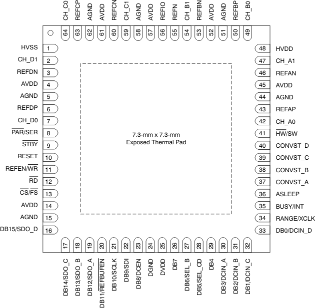
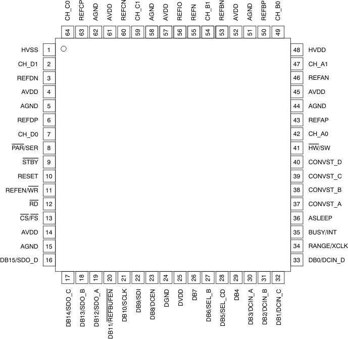
6 Pin Configuration and Functions
RGC Package
64-Pin VQFN
Top View
PM Package
64-Pin LQFP
Top View
Pin Functions
| PIN | TYPE(1) | DESCRIPTION | ||
|---|---|---|---|---|
| NAME | NO. | PARALLEL INTERFACE (PAR/SER = 0) | SERIAL INTERFACE (PAR/SER = 1) | |
| AGND | 5, 15, 44, 51, 58, 62 | P | Analog ground; connect to the analog ground plane. | |
| ASLEEP | 36 | DI | Auto-sleep enable input. When low, the device operates in normal mode. When high, the device functions in auto-sleep mode where the hold mode and the actual conversion is activated six conversion clock (tCCLK) cycles after issuing a conversion start using a CONVST_x. This mode is recommended to save power if the device runs at a lower data rate; see the Reset and Power-Down Modes section for more details. |
|
| AVDD | 4, 14, 45, 52, 57, 61 | P | Analog power supply. Decouple according to the Power Supply Recommendations section. |
|
| BUSY/INT | 35 | DO | When CONFIG bit C27 = 0 (BUSY/INT), this pin is a converter busy status output. This pin transitions high when a conversion is started and transitions low for a single conversion clock cycle (tCCLK) whenever a channel pair conversion is completed and stays low when the conversion of the last channel pair completes. When bit C27 = 1 (BUSY/INT in CONFIG), this pin is an interrupt output. This pin transitions high after a conversion completes and remains high until the next read access. This mode can only be used if all eight channels are sampled simultaneously (all CONVST_x tied together). The polarity of the BUSY/INT output can be changed using the C26 bit (BUSY L/H) in the Configuration register. |
|
| CH_A0 | 42 | AI | Analog input of channel A0; channel A is the master channel pair that is always active. The input voltage range is controlled by the RANGE pin in hardware mode or by Configuration register (CONFIG) bit C24 (RANGE_A) in software mode. In cases where channel pairs of the device are used at different data rates, channel pair A must always run at the highest data rate. |
|
| CH_A1 | 47 | AI | Analog input of channel A1; channel A is the master channel pair that is always active. The input voltage range is controlled by the RANGE pin in hardware mode or by CONFIG bit C24 (RANGE_A) in software mode. In cases where channel pairs of the device are used at different data rates, channel pair A must always run at the highest data rate. |
|
| CH_B0 | 49 | AI | Analog input of channel B0. The input voltage range is controlled by the RANGE pin in hardware mode or by CONFIG bit C23 (RANGE_B) in software mode. | |
| CH_B1 | 54 | AI | Analog input of channel B1. The input voltage range is controlled by the RANGE pin in hardware mode or by CONFIG bit C23 (RANGE_B) in software mode. | |
| CH_C0 | 64 | AI | Analog input of channel C0. The input voltage range is controlled by the RANGE pin in hardware mode or by CONFIG bit C21 (RANGE_C) in software mode. | |
| CH_C1 | 59 | AI | Analog input of channel C1. The input voltage range is controlled by the RANGE pin in hardware mode or by CONFIG bit C21 (RANGE_C) in software mode. | |
| CH_D0 | 7 | AI | Analog input of channel D0.The input voltage range is controlled by the RANGE pin in hardware mode or by CONFIG bit C19 (RANGE_D) in software mode. This pin can be powered down using CONFIG bit C18 (PD_D) in software mode. | |
| CH_D1 | 2 | AI | Analog input of channel D1.The input voltage range is controlled by the RANGE pin in hardware mode or by CONFIG bit C19 (RANGE_D) in software mode. This pin can be powered down using CONFIG bit C18 (PD_D) in software mode. | |
| CONVST_A | 37 | DI | Conversion start of channel pair A. The rising edge of this signal initiates simultaneous conversion of analog signals at inputs CH_A[1:0]. This signal resets the internal channel state machine that causes the data output to start with conversion results of channel A0 with the next read access. |
|
| CONVST_B | 38 | DI | Conversion start of channel pair B. The rising edge of this signal initiates simultaneous conversion of analog signals at inputs CH_B[1:0]. |
|
| CONVST_C | 39 | DI | Conversion start of channel pair C. The rising edge of this signal initiates simultaneous conversion of analog signals at inputs CH_C[1:0]. |
|
| CONVST_D | 40 | DI | Conversion start of channel pair D. The rising edge of this signal initiates simultaneous conversion of analog signals at inputs CH_D[1:0]. |
|
| CS/FS | 13 | DI, DI | Chip-select input. When low, the parallel interface is enabled. When high, the interface is disabled. |
Frame synchronization. The FS falling edge controls the frame transfer. |
| DB0/DCIN_D | 33 | DIO, DI | Data bit 0 (LSB) input/output | When DCEN = 1 and SEL_CD = 1, this pin is the daisy-chain data input for SDO_D of the previous device in the chain. When DCEN = 0, connect to DGND. |
| DB1/DCIN_C | 32 | DIO, DI | Data bit 1 input/output | When DCEN = 1 and SEL_CD = 1, this pin is the daisy-chain data input for SDO_C of the previous device in the chain. When DCEN = 0, connect to DGND. |
| DB2/DCIN_B | 31 | DIO, DI | Data bit 2 input/output | When DCEN = 1 and SEL_B = 1, this pin is the daisy-chain data input for SDO_B of the previous device in the chain. When DCEN = 0, connect to DGND. |
| DB3/DCIN_A | 30 | DIO, DI | Data bit 3 input/output | When DCEN = 1, this pin is the daisy-chain data input for SDO_A of the previous device in the chain. When DCEN = 0, connect to DGND. |
| DB4 | 29 | DIO | Data bit 4 input/output | Connect to DGND |
| DB5/SEL_CD | 28 | DIO, DI | Data bit 5 input/output | Select SDO_C and SDO_D input. When high, data from channel pair C are available on SDO_C and data from channel pair D are available on SDO_D. When low and SEL_B = 1, data from channel pairs A and C are available on SDO_A and data from channel pairs B and D are available on SDO_B. When low and SEL_B = 0, data from all eight channels are available on SDO_A. |
| DB6/SEL_B | 27 | DIO, DI | Data bit 6 input/output | Select SDO_B input. When low, SDO_B is disabled and data from all eight channels are only available through SDO_A. When high and SEL_CD = 0, data from channel pairs B and D are available on SDO_B. When SEL_CD = 1, data from channel pair B are available on SDO_B. |
| DB7 | 26 | DIO | Data bit 7 input/output | Must be connected to DGND |
| DB8/DCEN | 23 | DIO, DI | Data bit 8 input/output | Daisy-chain enable input. When high, DB[3:0] serve as daisy-chain inputs DCIN_[A:D]. If daisy-chain mode is not used, connect to DGND. |
| DB9/SDI | 22 | DIO, DI | Data bit 9 input/output | Hardware mode (HW/SW = 0): connect to DGND. Software mode (HW/SW = 1): serial data input. |
| DB10/SCLK | 21 | DIO, DI | Data bit 10 input/output | Serial interface clock input. |
| DB11/ REFBUFEN |
20 | DIO, DI | Data bit 11 input/output. Output is MSB for the ADS8528. |
Hardware mode (HW/SW = 0): reference buffer enable input. When low, all internal reference buffers are enabled (mandatory if internal reference is used). When high, all reference buffers are disabled. |
| Software mode (HW/SW = 1): connect to DGND or DVDD. The internal reference buffers are controlled by CONFIG bit C14 (REFBUFEN). |
||||
| DB12/SDO_A | 19 | DIO, DO | Data bit 12 input/output. Output is sign extension for the ADS8528. |
Data output for channel pair A. When SEL_CD = 0, data from channel pair C are also available on this output. When SEL_CD = 0 and SEL_B = 0, SDO_A functions as single data output for all eight channels. |
| DB13/SDO_B | 18 | DIO, DO | Data bit 13 input/output. Output is sign extension for the ADS8528 and MSB for the ADS8548. |
When SEL_B = 1, this pin is the data output for channel pair B. When SEL_B = 0, tie this pin to DGND. When SEL_CD = 0, data from channel pair D are also available on this output. |
| DB14/SDO_C | 17 | DIO, DO | Data bit 14 input/output. Output is sign extension for the ADS8528 and ADS8548. |
When SEL_CD = 1, this pin is the data output for channel pair C. When SEL_CD = 0, tie this pin to DGND. |
| DB15/SDO_D | 16 | DIO, DO | Data bit 15 (MSB) input/output. Output is sign extension for the ADS8528 and ADS8548. |
When SEL_CD = 1, this pin is the data output for channel pair D. When SEL_CD = 0, tie this pin to DGND. |
| DGND | 24 | P | Buffer I/O ground, connect to digital ground plane | |
| DVDD | 25 | P | Buffer I/O supply, connect to digital supply. Decouple according to the Power Supply Recommendations section. |
|
| HVDD | 48 | P | Positive supply voltage for the analog inputs. Decouple according to the Power Supply Recommendations section. |
|
| HVSS | 1 | P | Negative supply voltage for the analog inputs. Decouple according to the Power Supply Recommendations section. |
|
| HW/SW | 41 | DI | Mode selection input. When low, hardware mode is selected and the device functions according to the settings of the external pins. When high, software mode is selected and the device is configured by writing to the Configuration register (CONFIG). |
|
| PAR/SER | 8 | DI | Interface mode selection input. When low, the parallel interface is selected. When high, the serial interface is enabled. |
|
| RANGE/XCLK | 34 | DI/DI/DO | Hardware mode (HW/SW = 0): analog input voltage range select input. When low, the analog input voltage range is ±4 VREF. When high, the analog input voltage range is ±2 VREF. |
|
| Software mode (HW/SW = 1): this pin is an external conversion clock input if CONFIG bit C29 = 1 (CLKSEL); or an internal conversion clock output if CONFIG bit C28 = 1 (CLKOUT_EN). If this pin is not used, connect to DGND. |
||||
| RD | 12 | DI/DI | Read data input. When low, the parallel data output is enabled (if CS = 0). When high, the data output is disabled. |
Must be connected to DGND. |
| REFAN | 46 | AI | Decoupling capacitor input for reference of channel pair A. Connect to the decoupling capacitor and AGND according to the Power Supply Recommendations section. |
|
| REFAP | 43 | AI | Decoupling capacitor input for reference of channel pair A. Connect to the decoupling capacitor according to the Power Supply Recommendations section. |
|
| REFBN | 53 | AI | Decoupling capacitor input for reference of channel pair B. Connect to the decoupling capacitor and AGND according to the Power Supply Recommendations section. |
|
| REFBP | 50 | AI | Decoupling capacitor input for reference of channel pair B. Connect to the decoupling capacitor according to the Power Supply Recommendations section. |
|
| REFCN | 60 | AI | Decoupling capacitor input for reference of channel pair C. Connect to the decoupling capacitor and AGND according to the Power Supply Recommendations section. |
|
| REFCP | 63 | AI | Decoupling capacitor input for reference of channel pair C. Connect to the decoupling capacitor according to the Power Supply Recommendations section. |
|
| REFDN | 3 | AI | Decoupling capacitor input for reference of channel pair D. Connect to the decoupling capacitor and AGND according to the Power Supply Recommendations section. |
|
| REFDP | 6 | AI | Decoupling capacitor input for the channel pair D reference. Connect to the decoupling capacitor according to the Power Supply Recommendations section. |
|
| REFEN/WR | 11 | DI/DI | Hardware mode (HW/SW = 0): internal reference enable input. When high, the internal reference is enabled (the reference buffers are also enabled). When low, the internal reference is disabled and an external reference is applied at REFIO. |
Hardware mode (HW/SW = 0): internal reference enable input. When high, the internal reference is enabled (the reference buffers are also enabled). When low, the internal reference is disabled and an external reference is applied at REFIO. |
| Software mode (HW/SW = 1): write input. The parallel data input is enabled when CS and WR are low. The internal reference is enabled by CONFIG bit C15 (REFEN). |
Software mode (HW/SW = 1): connect to DGND or DVDD. The internal reference is enabled by CONFIG bit C15 (REFEN). | |||
| REFIO | 56 | AIO | Reference voltage input/output. The internal reference is enabled by the REFEN/WR pin in hardware mode or by CONFIG bit C15 (REFEN) in software mode. The output value is controlled by the internal digital-to-analog converter (DAC), CONFIG bits C[9:0]. Connect to a decoupling capacitor according to the Power Supply Recommendations section. |
|
| REFN | 55 | AI | Negative reference input/output pin. Connect to a decoupling capacitor and AGND according to the Power Supply Recommendations section. |
|
| RESET | 10 | DI | Reset input, active high. This pin aborts any ongoing conversions and resets the internal Configuration register (CONFIG) to 000003FFh. A valid reset pulse must be at least 50 ns long. |
|
| STBY | 9 | DI | Hardware mode (HW/SW = 0): standby mode input. When low, the entire device is powered down (including the internal conversion clock source and reference). When high, the device operates in normal mode. |
|
| Software mode (HW/SW = 1): connect to DGND or DVDD. The standby mode can be activated using CONFIG bit C25 (STBY). |
||||
(1) AI = analog input; AIO = analog input/output; DI = digital input; DIO = digital input/output; DO = digital output; and P = power supply.
7 Specifications
7.1 Absolute Maximum Ratings
over operating free-air temperature range (unless otherwise noted)(1)(1) Stresses beyond those listed under Absolute Maximum Ratings may cause permanent damage to the device. These are stress ratings only, which do not imply functional operation of the device at these or any other conditions beyond those indicated under Recommended Operating Conditions. Exposure to absolute-maximum-rated conditions for extended periods may affect device reliability.
7.2 ESD Ratings
| VALUE | UNIT | |||
|---|---|---|---|---|
| V(ESD) | Electrostatic discharge | Human-body model (HBM), per ANSI/ESDA/JEDEC JS-001(1) | ±2500 | V |
| Charged-device model (CDM), per JEDEC specification JESD22-C101(2) | ±500 | |||
(1) JEDEC document JEP155 states that 500-V HBM allows safe manufacturing with a standard ESD control process.
(2) JEDEC document JEP157 states that 250-V CDM allows safe manufacturing with a standard ESD control process.
7.3 Recommended Operating Conditions
over operating free-air temperature range (unless otherwise noted)| MIN | NOM | MAX | UNIT | ||
|---|---|---|---|---|---|
| AVDD | Analog supply voltage | 4.5 | 5.0 | 5.5 | V |
| DVDD | Buffer I/O supply voltage | 2.7 | 3.3 | 5.5 | V |
| HVDD | Input positive supply voltage | 5.0 | 15.0 | 16.5 | V |
| HVSS | Input negative supply voltage | –16.5 | –15.0 | –5.0 | V |
| TA | Operating ambient temperature range | –40 | 25 | 125 | °C |
7.4 Thermal Information
| THERMAL METRIC(1) | ADS85x8 | UNIT | ||
|---|---|---|---|---|
| RGC (VQFN) | PM (LQFP) | |||
| 64 PINS | 64 PINS | |||
| RθJA | Junction-to-ambient thermal resistance | 22 | 48.5 | °C/W |
| RθJC(top) | Junction-to-case (top) thermal resistance | 9.0 | 9.4 | °C/W |
| RθJB | Junction-to-board thermal resistance | 3.6 | 21.9 | °C/W |
| ψJT | Junction-to-top characterization parameter | 0.1 | 0.3 | °C/W |
| ψJB | Junction-to-board characterization parameter | 2.9 | 21.4 | °C/W |
| RθJC(bot) | Junction-to-case (bottom) thermal resistance | 0.3 | n/a | °C/W |
(1) For more information about traditional and new thermal metrics, see the Semiconductor and IC Package Thermal Metrics application report, SPRA953.
7.5 Electrical Characteristics: General
All minimum and maximum specifications are at TA = –40°C to +125°C, specified supply voltage range, VREF = 2.5 V (internal), VIN = ±10 V, and fDATA = max, unless otherwise noted. Typical values are at TA = 25°C, HVDD = 15 V, HVSS = –15 V, AVDD = 5 V, and DVDD = 3.3 V.| PARAMETER | TEST CONDITIONS | MIN | TYP | MAX | UNIT | |
|---|---|---|---|---|---|---|
| ANALOG INPUT | ||||||
| CHXX | Bipolar full-scale range | RANGE pin, RANGE bit = 0 | –4 VREF | 4 VREF | V | |
| RANGE pin, RANGE bit = 1 | –2 VREF | 2 VREF | ||||
| Input capacitance | Input range = ±4 VREF | 10 | pF | |||
| Input range = ±2 VREF | 20 | |||||
| Input leakage current | No ongoing conversion | –1 | 1 | μA | ||
| Aperture delay | 5 | ns | ||||
| Aperture delay matching | Common CONVST for all channels | 100 | ps | |||
| Aperture jitter | 50 | ps | ||||
| PSRR | Power-supply rejection ratio | At output code FFFFh, related to HVDD and HVSS | –78 | dB | ||
| REFERENCE VOLTAGE OUTPUT (REFOUT) | ||||||
| VREF | Reference voltage | 2.5-V operation, REFDAC = 3FFh | 2.485 | 2.5 | 2.515 | V |
| 2.5-V operation, REFDAC = 3FFh at 25°C | 2.496 | 2.5 | 2.504 | |||
| 3.0-V operation, REFDAC = 3FFh | 2.985 | 3.0 | 3.015 | |||
| 3.0-V operation, REFDAC = 3FFh at 25°C | 2.995 | 3.0 | 3.005 | |||
| dVREF/dT | Reference voltage drift | ±10 | ppm/°C | |||
| PSRR | Power-supply rejection ratio | At output code FFFFh, related to AVDD | –77 | dB | ||
| IREFOUT | Output current | At dc current | –2 | 2 | mA | |
| IREFSC | Short-circuit current(1) | 50 | mA | |||
| tREFON | Turn-on settling time | 10 | ms | |||
| External load capacitance | At REF_xP, REF_xN pins | 4.7 | 10 | μF | ||
| At REFIO pin | 100 | 470 | nF | |||
| REFDAC | Tuning range | Internal reference output voltage range | 0.2 VREF | VREF | V | |
| REFDAC resolution | 10 | Bits | ||||
| DNLDAC | REFDAC differential nonlinearity | –1 | ±0.1 | 1 | LSB | |
| INLDAC | REFDAC integral nonlinearity | –2 | ±0.1 | 2 | LSB | |
| VOSDAC | REFDAC offset error | VREF = 0.5 V (DAC = 0CDh) | –4 | ±0.65 | 4 | LSB |
| REFERENCE VOLTAGE INPUT (REFIN) | ||||||
| VREFIN | Reference input voltage | 0.5 | 2.5 | 3.025 | V | |
| Input resistance | 100 | MΩ | ||||
| Input capacitance | 5 | pF | ||||
| Reference input current | 1 | μA | ||||
| DIGITAL INPUTS(2) (CMOS with Schmitt-Trigger Logic Family) | ||||||
| High-level input voltage | 0.7 DVDD | DVDD + 0.3 | V | |||
| Low-level input voltage | DGND – 0.3 | 0.3 DVDD | V | |||
| Input current | VI = DVDD to DGND | –50 | 50 | nA | ||
| Input capacitance | 5 | pF | ||||
| DIGITAL OUTPUTS(2) | ||||||
| Output capacitance | 5 | pF | ||||
| Load capacitance | 30 | pF | ||||
| High-impedance-state output current | –50 | 50 | nA | |||
| Logic family | CMOS | |||||
| VOH | High-level output voltage | IOH = 100 μA | DVDD – 0.6 | V | ||
| VOL | Low-level output voltage | IOH = –100 μA | DGND + 0.4 | V | ||
| POWER-SUPPLY REQUIREMENTS | ||||||
| AVDD | Analog supply voltage | 4.5 | 5.0 | 5.5 | V | |
| DVDD | Buffer I/O supply voltage | 2.7 | 3.3 | 5.5 | V | |
| HVDD | Input positive supply voltage | 5.0 | 15.0 | 16.5 | V | |
| HVSS | Input negative supply voltage | –16.5 | –15.0 | –5.0 | V | |
| IAVDD | Analog supply current | ADS8528, fDATA = maximum | 37.9 | 50.1 | mA | |
| ADS8548, fDATA = maximum | 37.3 | 49.3 | ||||
| ADS8568, fDATA = maximum | 36.6 | 48.4 | ||||
| fDATA = 250 kSPS, auto-sleep mode | 20.3 | 30.0 | ||||
| fDATA = 200 kSPS, auto-sleep mode | 17 | |||||
| fDATA = 10 kSPS, normal operation | 30 | |||||
| fDATA = 10 kSPS, auto-sleep mode | 4.6 | |||||
| Auto-sleep mode, no ongoing conversion, internal conversion clock |
7.0 | |||||
| Power-down mode | 0.03 | |||||
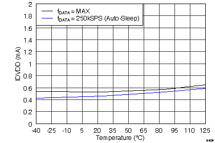
| IDVDD | Buffer I/O supply current | fDATA = maximum | 0.5 | 2.0 | mA | |
| fDATA = 250 kSPS | 0.5 | 1.4 | ||||
| fDATA = 200 kSPS | 0.5 | |||||
| fDATA = 10 kSPS | 0.4 | |||||
| Auto-sleep mode, no ongoing conversion, internal conversion clock |
0.35 | |||||
| Power-down mode | 0.01 | |||||
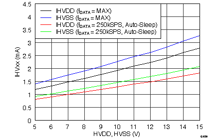
| IHVDD | Input positive supply current | ADS8528, fDATA = maximum | 3.0 | 4.2 | mA | |
| ADS8548, fDATA = maximum | 2.8 | 3.9 | ||||
| ADS8568, fDATA = maximum | 2.3 | 3.2 | ||||
| fDATA = 250 kSPS | 1.8 | 2.4 | ||||
| fDATA = 200 kSPS | 1.5 | |||||
| fDATA = 10 kSPS | 0.4 | |||||
| Auto-sleep mode, no ongoing conversion, internal conversion clock |
0.45 | |||||
| Power-down mode | 0.01 | |||||
| POWER-SUPPLY REQUIREMENTS (continued) | ||||||
| IHVSS | Input negative supply current | ADS8528, fDATA = maximum | 3.4 | 4.5 | mA | |
| ADS8548, fDATA = maximum | 3.3 | 4.4 | ||||
| ADS8568, fDATA = maximum | 2.7 | 3.6 | ||||
| fDATA = 250 kSPS | 2.1 | 2.6 | ||||
| fDATA = 200 kSPS | 1.7 | |||||
| fDATA = 10 kSPS | 0.4 | |||||
| Auto-sleep mode, no ongoing conversion, internal conversion clock |
0.35 | |||||
| Power-down mode | 0.01 | |||||
| Power dissipation(3) | ADS8528, fDATA = maximum | 287.1 | 430.1 | mW | ||
| ADS8548, fDATA = maximum | 279.7 | 419.1 | ||||
| ADS8568, fDATA = maximum | 259.7 | 389.4 | ||||
| fDATA = 250 kSPS, auto-sleep mode | 161.7 | 255.2 | ||||
| fDATA = 200 kSPS, auto-sleep mode | 151.2 | |||||
| fDATA = 10 kSPS, normal operation | 163.3 | |||||
| fDATA = 10 kSPS, auto-sleep mode | 36.3 | |||||
| Auto-sleep mode, no ongoing conversion, internal conversion clock |
53.6 | |||||
| Power-down mode | 0.6 | |||||
(1) Reference output current is not limited internally.
(2) Specified by design.
(3) Maximum power dissipation values are specified with HVDD = 15 V and HVSS = –15 V.
7.6 Electrical Characteristics: ADS8528
All minimum and maximum specifications are at TA = –40°C to +125°C, specified supply voltage range, VREF = 2.5 V (internal), VIN = ±10 V, and fDATA = max, unless otherwise noted. Typical values are at TA = 25°C, HVDD = 15 V, HVSS = –15 V, AVDD = 5 V, and DVDD = 3.3 V.| PARAMETER | TEST CONDITIONS | MIN | TYP | MAX | UNIT | |
|---|---|---|---|---|---|---|
| SAMPLING DYNAMICS | ||||||
| Conversion time | Internal conversion clock | 1.33 | μs | |||
| fDATA | Throughput rate | Serial interface, all four SDOx active | 480 | kSPS | ||
| Parallel interface | 650 | |||||
| DC ACCURACY | ||||||
| Resolution | 12 | Bits | ||||
| No missing codes | 12 | Bits | ||||
| INL | Integral linearity error(1) | –0.75 | ±0.2 | 0.75 | LSB | |
| DNL | Differential linearity error | –0.5 | ±0.2 | 0.5 | LSB | |
| Offset error | –1.5 | ±0.5 | 1.5 | mV | ||
| Offset error matching | –0.65 | 0.65 | mV | |||
| Offset error drift | ±3.5 | μV/°C | ||||
| Gain error | Referenced to voltage at REFIO | –0.5% | ±0.25% | 0.5% | ||
| Gain error matching | Between channels of any pair | –0.2% | 0.2% | |||
| Between any two channels | –0.4% | 0.4% | ||||
| Gain error drift | Referenced to voltage at REFIO | ±6 | ppm/°C | |||
| AC ACCURACY | ||||||
| SNR | Signal-to-noise ratio | At fIN = 10 kHz | 73 | 73.9 | dB | |
| SINAD | Signal-to-noise ratio + distortion | At fIN = 10 kHz | 73 | 73.8 | dB | |
| THD | Total harmonic distortion(2) | At fIN = 10 kHz | –89 | –84 | dB | |
| SFDR | Spurious-free dynamic range | At fIN = 10 kHz | 84 | 92 | dB | |
| Channel-to-channel isolation | At fIN = 10 kHz | 120 | dB | |||
| BW | –3-dB small-signal bandwidth | In 4-VREF mode | 48 | MHz | ||
| In 2-VREF mode | 24 | |||||
(1) Integral nonlinearity is defined as the maximum deviation from a straight line passing through the end-points of the ideal ADC transfer function expressed as the number of LSBs or percentage of the specified full-scale range.
(2) Calculated on the first nine harmonics of the input frequency.
7.7 Electrical Characteristics: ADS8548
All minimum and maximum specifications are at TA = –40°C to +125°C, specified supply voltage range, VREF = 2.5 V (internal), VIN = ±10 V, and fDATA = max, unless otherwise noted. Typical values are at TA = 25°C, HVDD = 15 V, HVSS = –15 V, AVDD = 5 V, and DVDD = 3.3 V.| PARAMETER | TEST CONDITIONS | MIN | TYP | MAX | UNIT | |
|---|---|---|---|---|---|---|
| SAMPLING DYNAMICS | ||||||
| Conversion time | Internal conversion clock | 1.45 | μs | |||
| fDATA | Throughput rate | Serial interface, all four SDOx active | 450 | kSPS | ||
| Parallel interface | 600 | |||||
| DC ACCURACY | ||||||
| Resolution | 14 | Bits | ||||
| No missing codes | 14 | Bits | ||||
| INL | Integral linearity error(1) | –1 | ±0.5 | 1 | LSB | |
| DNL | Differential linearity error | –1 | ±0.25 | 1 | LSB | |
| Offset error | –1.5 | ±0.5 | 1.5 | mV | ||
| Offset error matching | –0.65 | 0.65 | mV | |||
| Offset error drift | ±3.5 | μV/°C | ||||
| Gain error | Referenced to voltage at REFIO | –0.5% | ±0.25% | 0.5% | ||
| Gain error matching | Between channels of any pair | –0.2% | 0.2% | |||
| Between any two channels | –0.4% | 0.4% | ||||
| Gain error drift | Referenced to voltage at REFIO | ±6 | ppm/°C | |||
| AC ACCURACY | ||||||
| SNR | Signal-to-noise ratio | At fIN = 10 kHz | 84 | 85 | dB | |
| SINAD | Signal-to-noise ratio + distortion | At fIN = 10 kHz | 83 | 84 | dB | |
| THD | Total harmonic distortion(2) | At fIN = 10 kHz | –91 | –86 | dB | |
| SFDR | Spurious-free dynamic range | At fIN = 10 kHz | 86 | 92 | dB | |
| Channel-to-channel isolation | At fIN = 10 kHz | 120 | dB | |||
| BW | –3-dB small-signal bandwidth | In 4-VREF mode | 48 | MHz | ||
| In 2-VREF mode | 24 | |||||
(1) Integral nonlinearity is defined as the maximum deviation from a straight line passing through the end-points of the ideal ADC transfer function expressed as the number of LSBs or percentage of the specified full-scale range.
(2) Calculated on the first nine harmonics of the input frequency.
7.8 Electrical Characteristics: ADS8568
All minimum and maximum specifications are at TA = –40°C to +125°C, specified supply voltage range, VREF = 2.5 V (internal), VIN = ±10 V, and fDATA = max, unless otherwise noted. Typical values are at TA = 25°C, HVDD = 15 V, HVSS = –15 V, AVDD = 5 V, and DVDD = 3.3 V.| PARAMETER | TEST CONDITIONS | MIN | TYP | MAX | UNIT | |
|---|---|---|---|---|---|---|
| SAMPLING DYNAMICS | ||||||
| Conversion time | Internal conversion clock | 1.7 | μs | |||
| fDATA | Throughput rate | Serial interface, all four SDOx active | 400 | kSPS | ||
| Parallel interface | 510 | |||||
| DC ACCURACY | ||||||
| Resolution | 16 | Bits | ||||
| No missing codes | 16 | Bits | ||||
| INL | Integral linearity error(1) | At TA = –40°C to +85°C, VQFN package (RGC) | –3 | ±1.5 | 3 | LSB |
| At TA = –40°C to +125°C, VQFN package (RGC) | –4 | ±1.5 | 4 | |||
| At TA = –40°C to +85°C, LQFP package (PM) | –4 | ±1.5 | 4 | |||
| At TA = –40°C to +125°C, LQFP package (PM) | –4.5 | ±1.5 | 4.5 | |||
| DNL | Differential linearity error | At TA = –40°C to +85°C | –1 | ±0.75 | 1.75 | LSB |
| At TA = –40°C to +125°C | –1 | ±0.75 | 2 | |||
| Offset error | –1.5 | ±0.5 | 1.5 | mV | ||
| Offset error matching | –0.65 | 0.65 | mV | |||
| Offset error drift | ±3.5 | μV/°C | ||||
| Gain error | Referenced to voltage at REFIO | –0.5% | ±0.25% | 0.5% | ||
| Gain error matching | Between channels of any pair | –0.2% | 0.2% | |||
| Between any two channels | –0.4% | 0.4% | ||||
| Gain error drift | Referenced to voltage at REFIO | ±6 | ppm/°C | |||
| AC ACCURACY | ||||||
| SNR | Signal-to-noise ratio | At fIN = 10 kHz, TA = –40°C to +85°C | 90 | 91.5 | dB | |
| At fIN = 10 kHz, TA = –40°C to +125°C | 89 | 91.5 | ||||
| SINAD | Signal-to-noise ratio + distortion | At fIN = 10 kHz, TA = –40°C to +85°C | 87 | 90 | dB | |
| At fIN = 10 kHz, TA = –40°C to +125°C | 86.5 | 90 | ||||
| THD | Total harmonic distortion(2) | At fIN = 10 kHz, TA = –40°C to +85°C | –94 | –90 | dB | |
| At fIN = 10 kHz, TA = –40°C to +125°C | –94 | –89.5 | ||||
| SFDR | Spurious-free dynamic range | At fIN = 10 kHz, TA = –40°C to +85°C | 90 | 95 | dB | |
| At fIN = 10 kHz, TA = –40°C to +125°C | 89.5 | 95 | ||||
| Channel-to-channel isolation | At fIN = 10 kHz | 120 | dB | |||
| BW | –3-dB small-signal bandwidth | In 4-VREF mode | 48 | MHz | ||
| In 2-VREF mode | 24 | |||||
(1) Integral nonlinearity is defined as the maximum deviation from a straight line passing through the end-points of the ideal ADC transfer function expressed as the number of LSBs or percentage of the specified full-scale range.
7.9 Serial Interface Timing Requirements
over recommended operating free-air temperature range (TA), AVDD = 5 V, and DVDD = 2.7 V to 5.5 V (unless otherwise noted)(1)| MIN | NOM | MAX | UNIT | |||
|---|---|---|---|---|---|---|
| tSCVX | CONVST_x high to XCLK rising edge setup time (CLKSEL = 1) |
6 | ns | |||
| tXCLK | External conversion clock period | ADS8528 | 66.67 | ns | ||
| ADS8548 | 72.46 | |||||
| ADS8568 | 85.11 | |||||
| External conversion clock frequency | ADS8528 | 1 | 15.0 | MHz | ||
| ADS8548 | 1 | 13.8 | ||||
| ADS8568 | 1 | 11.75 | ||||
| External conversion clock duty cycle | 40% | 60% | ||||
| tCVL | CONVST_x low time | 20 | ns | |||
| tACQ | Acquisition time | 280 | ns | |||
| Clock cycles per conversion | ADS85x8, tCCLK or tXCLK |
19 | 20 | Cycles | ||
| tCONV | Conversion time | ADS8528, CLKSEL = 0 | 1.33 | μs | ||
| ADS8548, CLKSEL = 0 | 1.45 | |||||
| ADS8568, CLKSEL = 0 | 1.7 | |||||
| tDCVB | CONVST_x high to BUSY high delay | 25 | ns | |||
| tBUFS | BUSY low to FS low time | ADS85x8, CLKSEL = 1 | 0 | ns | ||
| ADS8528, CLKSEL = 0(2) | 67 | |||||
| ADS8548, CLKSEL = 0(2) | 73 | |||||
| ADS8568, CLKSEL = 0(2) | 86 | |||||
| tFSCV | Bus access finished to next conversion start time | ADS8528 | 0 | ns | ||
| ADS8548 | 20 | |||||
| ADS8568 | 40 | |||||
| tSCLK | Serial clock period | 0.022 | 10 | μs | ||
| Serial clock frequency | 0.1 | 45 | MHz | |||
| Serial clock duty cycle | 40% | 60% | ||||
| tDMSB | FS low to MSB valid delay | 12 | ns | |||
| tHDO | Output data to SCLK falling edge hold time | 5 | ns | |||
| tPDDO | SCLK falling edge to new data valid propagation delay | 17 | ns | |||
| tDTRI | FS high to SDO_x three-state delay | 10 | ns | |||
| tSUDI | Input data to SCLK falling edge setup time | 3 | ns | |||
| tHDI | Input data to SCLK falling edge hold time | 5 | ns | |||
(1) All input signals are specified with tR = tF = 1.5 ns (10% to 90% of DVDD) and timed from a voltage level of (VIL + VIH) / 2.
(2) The device runs with an internal conversion clock. Data can be retrieved after the maximum conversion time tCONV(max), independently from the BUSY signal. When referring the data readout to the falling edge of the BUSY signal, tBUFS(min) must be taken into account (see the Data Readout and BUSY/INT Signal section).
7.10 Parallel Interface Timing Requirements (Read Access)
over recommended operating free-air temperature range (TA), AVDD = 5 V, and DVDD = 2.7 V to 5.5 V (unless otherwise noted)(1)| MIN | NOM | MAX | UNIT | |||
|---|---|---|---|---|---|---|
| tCVL | CONVST_x low time | 20 | ns | |||
| tACQ | Acquisition time | 280 | ns | |||
| Clock cycles per conversion | ADS85x8, tCCLK or tXCLK | 19 | 20 | Cycles | ||
| tCONV | Conversion time | ADS8528, CLKSEL = 0 | 1.33 | µs | ||
| ADS8548, CLKSEL = 0 | 1.45 | |||||
| ADS8568, CLKSEL = 0 | 1.7 | |||||
| tDCVB | CONVST_x high to BUSY high delay | 25 | ns | |||
| tBUCS | BUSY low to CS low time | ADS85x8, CLKSEL = 1 | 0 | ns | ||
| ADS8528, CLKSEL = 0(3) | 67 | |||||
| ADS8548, CLKSEL = 0(3) | 73 | |||||
| ADS8568, CLKSEL = 0(3) | 86 | |||||
| tCSCV | Bus access finished to next conversion start time(2) | ADS8528 | 0 | ns | ||
| ADS8548 | 20 | |||||
| ADS8568 | 40 | |||||
| tCSRD | CS low to RD low time | 0 | ns | |||
| tRDCS | RD high to CS high time | 0 | ns | |||
| tRDL | RD pulse duration | 20 | ns | |||
| tRDH | Minimum time between two read accesses | 2 | ns | |||
| tPDDO | RD or CS falling edge to data valid propagation delay | 15 | ns | |||
| tHDO | Output data to RD or CS rising edge hold time | 5 | ns | |||
| tDTRI | CS high to DB[15:0] three-state delay | 10 | ns | |||
(1) All input signals are specified with tR = tF = 1.5 ns (10% to 90% of DVDD) and timed from a voltage level of (VIL + VIH) / 2.
(2) See the CS signal or RD, whichever occurs first.
(3) The device runs with an internal conversion clock. Data can be retrieved after the maximum conversion time tCONV(max), independently from the BUSY signal. When referring the data readout to the falling edge of the BUSY signal, tBUCS(min) must be taken into account (see the Data Readout and BUSY/INT Signal section).
7.11 Parallel Interface Timing Requirements (Write Access)
over recommended ambient temperature range (TA), AVDD = 5 V, and DVDD = 2.7 V to 5.5 V (unless otherwise noted)(1)| MIN | NOM | MAX | UNIT | ||
|---|---|---|---|---|---|
| tCSWR | CS low to WR low time | 0 | ns | ||
| tWRL | WR low pulse duration | 15 | ns | ||
| tWRH | Minimum time between two write accesses | 10 | ns | ||
| tWRCS | WR high to CS high time | 0 | ns | ||
| tSUDI | Output data to WR rising edge setup time | 5 | ns | ||
| tHDI | Data output to WR rising edge hold time | 5 | ns | ||
(1) All input signals are specified with tR = tF = 1.5 ns (10% to 90% of DVDD) and timed from a voltage level of (VIL + VIH) / 2.
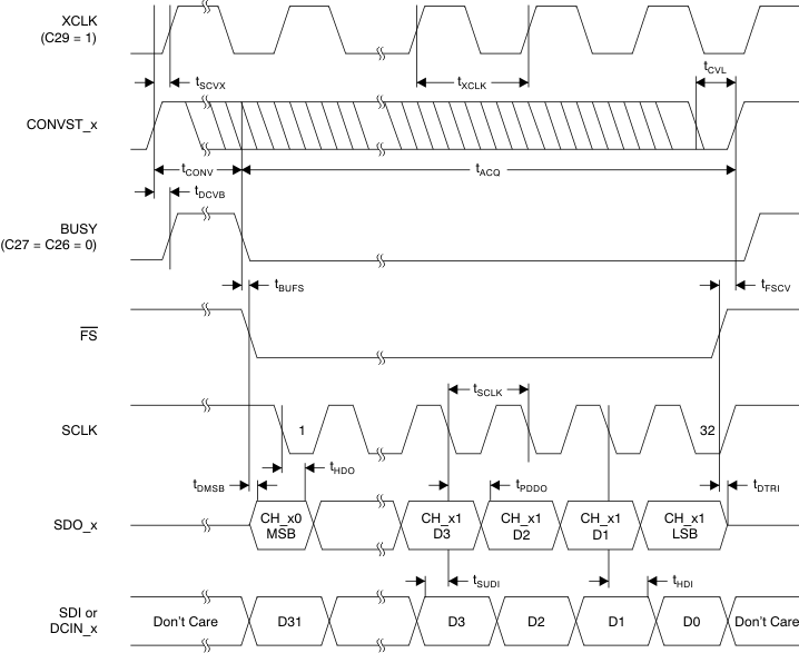 Figure 1. Serial Operation Timing Diagram (All Four SDO_x Active)
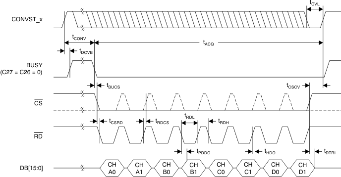 Figure 2. Parallel Read Access Timing Diagram
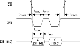 Figure 3. Parallel Write Access Timing Diagram
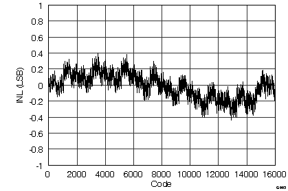
7.12 Typical Characteristics
graphs are valid for all devices of the family, at TA = 25°C, HVDD = 15 V, HVSS = –15 V, AVDD = 5 V, DVDD = 3.3 V, VREF = 2.5 V (internal), VIN = ±10 V, and fDATA = maximum (unless otherwise noted)
(ADS8528)
(ADS8548 ±10-VIN Range)

(ADS8548 ±10-VIN Range)
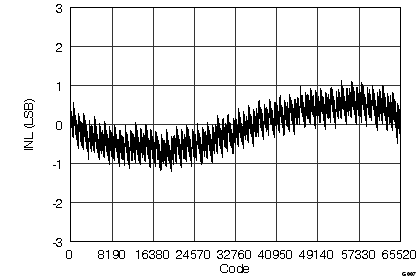
(ADS8568 ±10-VIN Range)

(ADS8568 ±10-VIN Range)
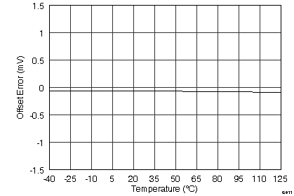
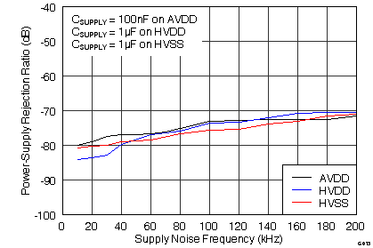
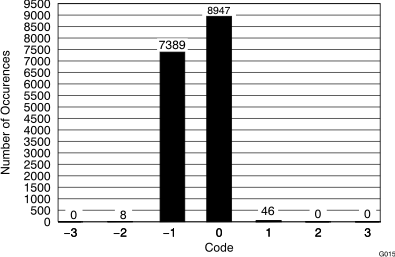
(ADS8568, 16390 Hits)
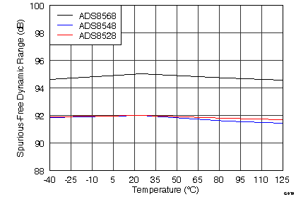
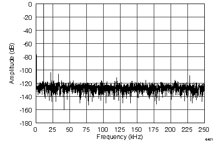
(ADS8568, 2048-Point FFT, fIN = 10 kHz, ±5-VIN Range)
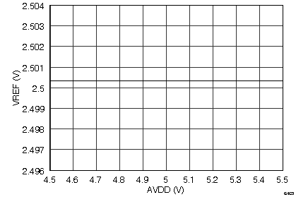
Analog Supply Voltage (2.5-V Mode)
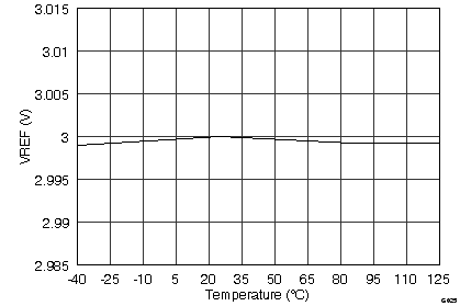
(3.0-V Mode)
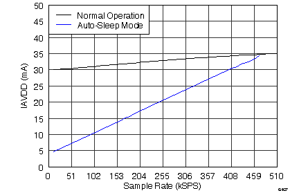
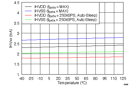
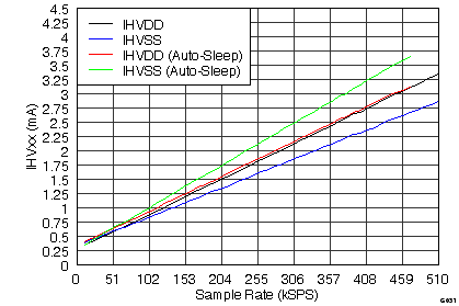
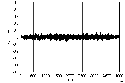
(ADS8528)
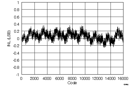
(ADS8548 ±5-VIN Range)
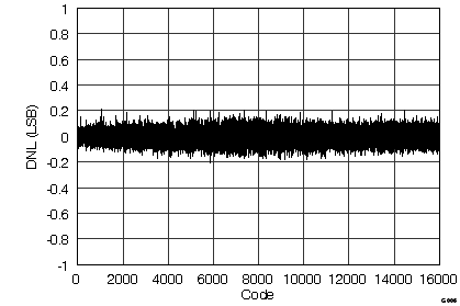
(ADS8548 ±5-VIN Range)
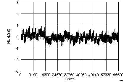
(ADS8568 ±5-VIN Range)
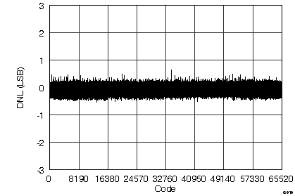
(ADS8568 ±5-VIN Range)
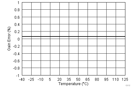
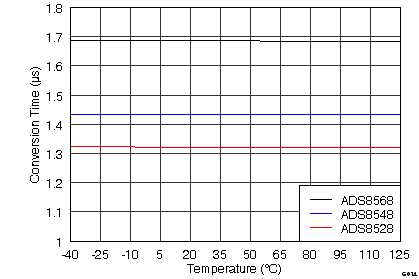

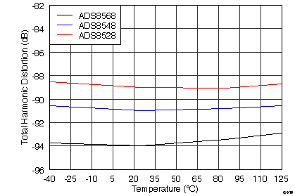
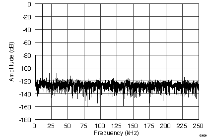
(ADS8568, 2048-Point FFT, fIN = 10 kHz, ±10-VIN Range)
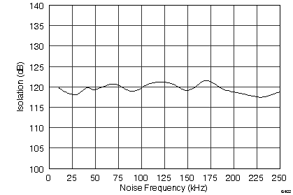
Input Noise Frequency
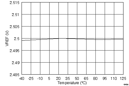
(2.5-V Mode)
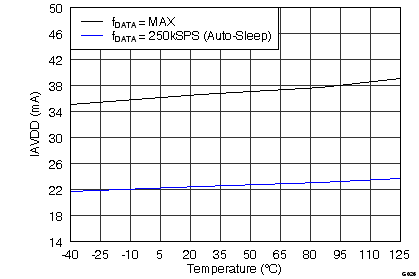
Input Supply Voltage