DATA SHEET
TPS7A4001 100V 输入电压、50mA 超高电压线性稳压器
本资源的原文使用英文撰写。 为方便起见,TI 提供了译文;由于翻译过程中可能使用了自动化工具,TI 不保证译文的准确性。 为确认准确性,请务必访问 ti.com 参考最新的英文版本(控制文档)。
1 特性
2 应用
- 由工业用总线(具有高电压瞬态)供电的微处理器、微控制器
- 工业自动化
- 电信基础设施
- 车用
- 以太网供电 (PoE)
- 发光二级管 (LED) 照明
- 偏置电源
3 说明
TPS7A4001 器件是一款能够耐受超高电压的线性稳压器,不仅融合了耐热增强型封装 (HVSSOP) 的优势,还能够承受持续直流电压或最高达 100V 的瞬态输入电压。
TPS7A4001 器件与任何高于 4.7µF 的输出电容以及高于 1µF 的输入电容搭配使用时均可保持稳定(过热和浪涌保护)。鉴于这款器件的封装 (HVSSOP) 小巧且可能使用的输出电容也较小,因此实现起来只需占用非常小的电路板空间。此外,TPS7A4001 器件还提供了一个与标准 CMOS 逻辑兼容的使能引脚 (EN),用以使能低电流关断模式。
TPS7A4001 器件内部具有热关断和电流限制功能,可在故障情况下保护系统。HVSSOP 封装的工作温度范围为 TJ = -40°C 至 125°C。
此外,TPS7A4001 器件非常适合在电信和工业 应用中利用中间电压轨生成低压电源;该器件不但能够提供一个充分稳压的电压轨,而且能够承受超高的快速电压瞬变并在其间保持稳压状态。这些 特性 相当于一套更为简单且经济高效的电气浪涌保护电路,因此受到 PoE、偏置电源和 LED 照明等 应用的青睐。
器件信息(1)
| 器件型号 | 封装 | 封装尺寸(标称值) |
|---|---|---|
| TPS7A4001 | HVSSOP (8) | 3.00mm x 5.00mm |
- 要了解所有可用封装,请见数据表末尾的可订购产品附录。
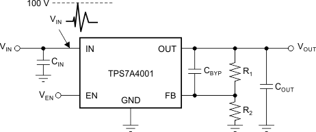
典型应用电路原理图
4 修订历史记录
Changes from A Revision (March 2011) to B Revision
- 已添加 ESD 额定值表,特性 描述部分,器件功能模式,应用和实施部分,电源相关建议部分,布局部分,器件和文档支持部分以及机械、封装和可订购信息部分。Go
- 已将封装从 MSOP-8 改为 HVSSOP。Go
- Changed TJ value for disabled mode operating mode from 165 to 170°CGo
- Changed value from 35 to 45°CGo
Changes from * Revision (March 2011) to A Revision
- 已将首页上的所有 105V 改为 100VGo
5 Pin Configuration and Functions
DGN Package
8-Pin HVSSOP
Top View

Pin Functions
| PIN | I/O | DESCRIPTION | |
|---|---|---|---|
| NAME | NO. | ||
| OUT | 1 | O | Regulator output. A capacitor > 4.7 µF must be tied from this pin to ground to assure stability. |
| FB | 2 | O | This pin is the input to the control-loop error amplifier. It is used to set the output voltage of the device. |
| NC | 3 | — | Not internally connected. This pin must either be left open or tied to GND. |
| 6 | |||
| 7 | |||
| GND | 4 | — | Ground |
| EN | 5 | I | This pin turns the regulator on or off. If VEN ≥ VEN_HI the regulator is enabled. If VEN ≤ VEN_LO, the regulator is disabled. If not used, the EN pin can be connected to IN. Make sure that VEN ≤ VIN at all times. |
| IN | 8 | I | Input supply |
| PowerPAD | — | — | Solder to printed-circuit-board (PCB) to enhance thermal performance. NOTE: The PowerPAD is internally connected to GND. Although it can be left floating, TI highly recommends connecting the PowerPAD to the GND plane. |
6 Specifications
6.1 Absolute Maximum Ratings
over operating junction temperature range (unless otherwise noted)(1)| MIN | MAX | UNIT | ||
|---|---|---|---|---|
| Voltage | IN pin to GND pin | –0.3 | 105 | V |
| OUT pin to GND pin | –0.3 | 105 | ||
| OUT pin to IN pin | –105 | 0.3 | ||
| FB pin to GND pin | –0.3 | 2 | ||
| FB pin to IN pin | –105 | 0.3 | ||
| EN pin to IN pin | –105 | 0.3 | ||
| EN pin to GND pin | –0.3 | 105 | ||
| Current | Peak output | Internally limited | ||
| Temperature | Operating virtual junction, TJ | –40 | 125 | °C |
| Storage, Tstg | –65 | 150 | ||
(1) Stresses beyond those listed under Absolute Maximum Ratings may cause permanent damage to the device. These are stress ratings only, which do not imply functional operation of the device at these or any other conditions beyond those indicated under Recommended Operating Conditions. Exposure to absolute-maximum-rated conditions for extended periods may affect device reliability.
6.2 ESD Ratings
| VALUE | UNIT | |||
|---|---|---|---|---|
| V(ESD) | Electrostatic discharge | Human-body model (HBM), per ANSI/ESDA/JEDEC JS-001(1) | ±2500 | V |
| Charged-device model (CDM), per JEDEC specification JESD22-C101(2) | ±500 | |||
(1) JEDEC document JEP155 states that 500-V HBM allows safe manufacturing with a standard ESD control process.
(2) JEDEC document JEP157 states that 250-V CDM allows safe manufacturing with a standard ESD control process.
6.3 Recommended Operating Conditions
over operating junction temperature range (unless otherwise noted)| MIN | NOM | MAX | UNIT | ||
|---|---|---|---|---|---|
| VIN | 7 | 100 | V | ||
| VOUT | 1.161 | 90 | V | ||
| VEN | 0 | 100 | V | ||
| IOUT | 0 | 50 | mA | ||
6.4 Thermal Information
| THERMAL METRIC(1) | TPS7A4001 | UNIT | |
|---|---|---|---|
| DGN (HVVSOP) | |||
| 8 PINS | |||
| RθJA | Junction-to-ambient thermal resistance | 66.7 | °C/W |
| RθJC(top) | Junction-to-case (top) thermal resistance | 54.1 | °C/W |
| RθJB | Junction-to-board thermal resistance | 38.1 | °C/W |
| ψJT | Junction-to-top characterization parameter | 2 | °C/W |
| ψJB | Junction-to-board characterization parameter | 37.8 | °C/W |
| RθJC(bot) | Junction-to-case (bottom) thermal resistance | 15.5 | °C/W |
(1) For more information about traditional and new thermal metrics, see the Semiconductor and IC Package Thermal Metrics application report, SPRA953.
6.5 Electrical Characteristics
At TJ = –40°C to 125°C, VIN = VOUT(NOM) + 2 V or VIN = 7 V (whichever is greater), VEN = VIN, IOUT = 100 µA, CIN = 1 μF, COUT = 4.7 μF, and FB tied to OUT, unless otherwise noted.| PARAMETER | TEST CONDITIONS | MIN | TYP | MAX | UNIT | |||
|---|---|---|---|---|---|---|---|---|
| VIN | Input voltage | 7 | 100 | V | ||||
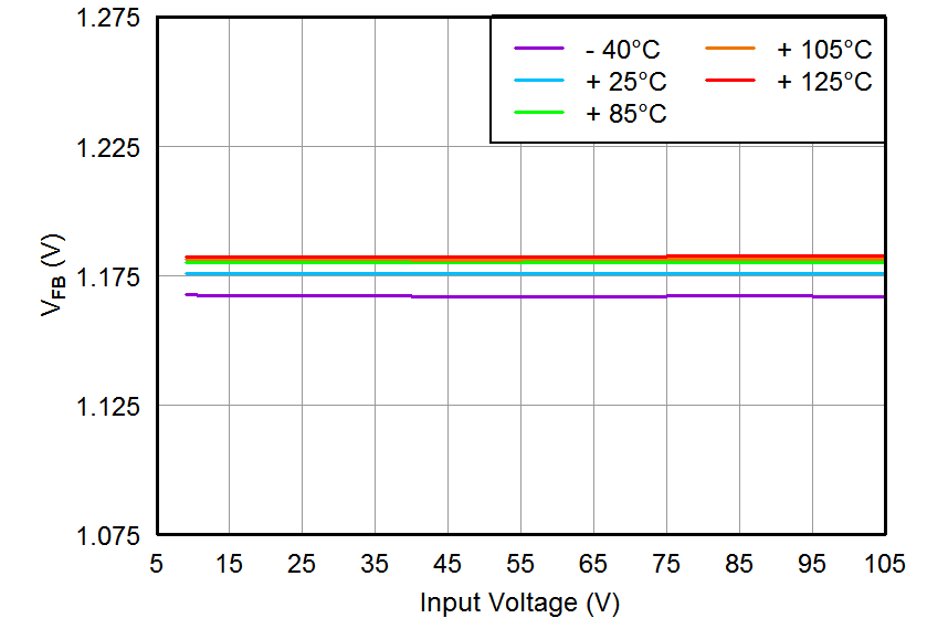
| VREF | Internal reference | TJ = 25°C, VFB = VREF, VIN = 9 V, IOUT = 25 mA | 1.161 | 1.173 | 1.185 | V | ||
| VOUT | Output voltage range(1) | VIN ≥ VOUT(NOM) + 2 V | VREF | 90 | V | |||
| Nominal accuracy | TJ = 25°C, VIN = 9 V, IOUT = 25 mA | –1 | 1 | %VOUT | ||||
| Overall accuracy | VOUT(NOM) + 2 V ≤ VIN ≤ 24 V(2)
100 µA ≤ IOUT ≤ 50 mA |
–2.5 | 2.5 | %VOUT | ||||
 |
Line regulation | 7 V ≤ VIN ≤ 100 V | 0.03 | %VOUT | ||||
 |
Load regulation | 100 µA ≤ IOUT ≤ 50 mA | 0.31 | %VOUT | ||||
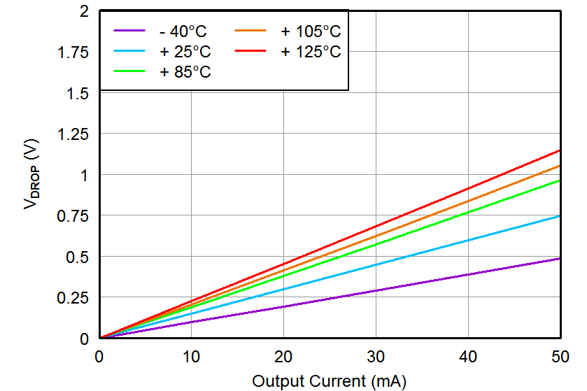
| VDO | Dropout voltage | VIN = 17 V, VOUT(NOM) = 18 V, IOUT = 20 mA | 290 | mV | ||||
| VIN = 17 V, VOUT(NOM) = 18 V, IOUT = 50mA | 0.78 | 1.3 | V | |||||
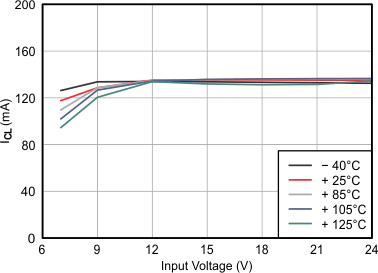
| ILIM | Current limit | VOUT = 90% VOUT(NOM), VIN = 7 V, TJ ≤ 85°C | 51 | 117 | 200 | mA | ||
| VOUT = 90% VOUT(NOM), VIN = 9 V | 51 | 128 | 200 | mA | ||||
| IGND | Ground current | 7 V ≤ VIN ≤ 100 V, IOUT = 0 mA | 25 | 65 | μA | |||
| IOUT = 50 mA | 25 | μA | ||||||
| ISHDN | Shutdown supply current | VEN = 0.4 V | 4.1 | 20 | μA | |||
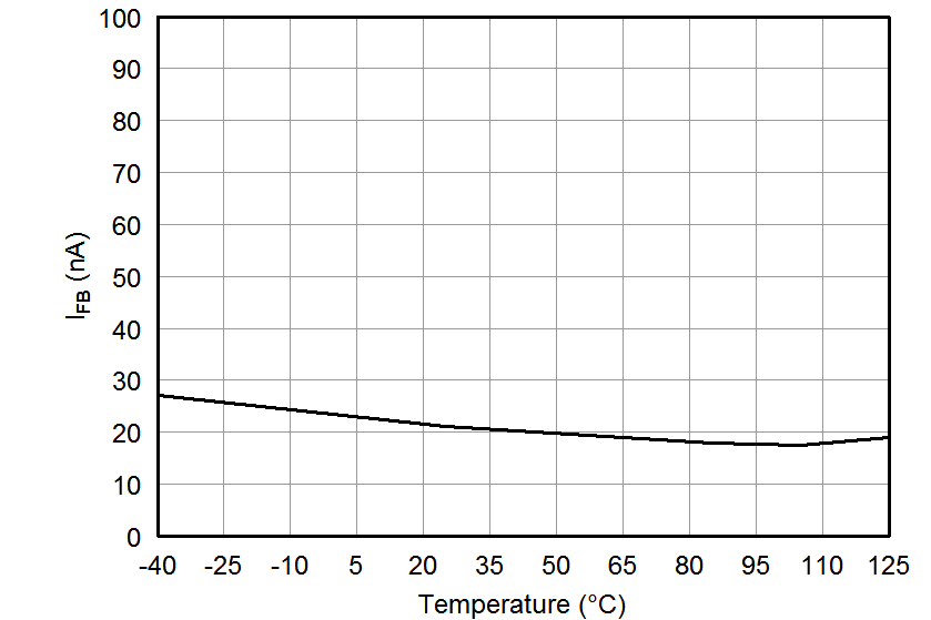
| IFB | Feedback current(3) | –0.1 | 0.01 | 0.1 | µA | |||
| IEN | Enable current | 7 V ≤ VIN ≤ 100 V, VIN = VEN | 0.02 | 1 | μA | |||
| VEN_HI | Enable high-level voltage | 1.5 | VIN | V | ||||
| VEN_LO | Enable low- level voltage | 0 | 0.4 | V | ||||
| VNOISE | Output noise voltage | VIN = 12 V, VOUT(NOM) = VREF, COUT = 10 μF, BW = 10 Hz to 100 kHz |
58 | μVRMS | ||||
| VIN = 12 V, VOUT(NOM) = 5 V, COUT = 10 μF, CBYP(4) = 10 nF, BW = 10 Hz to 100 kHz | 73 | μVRMS | ||||||
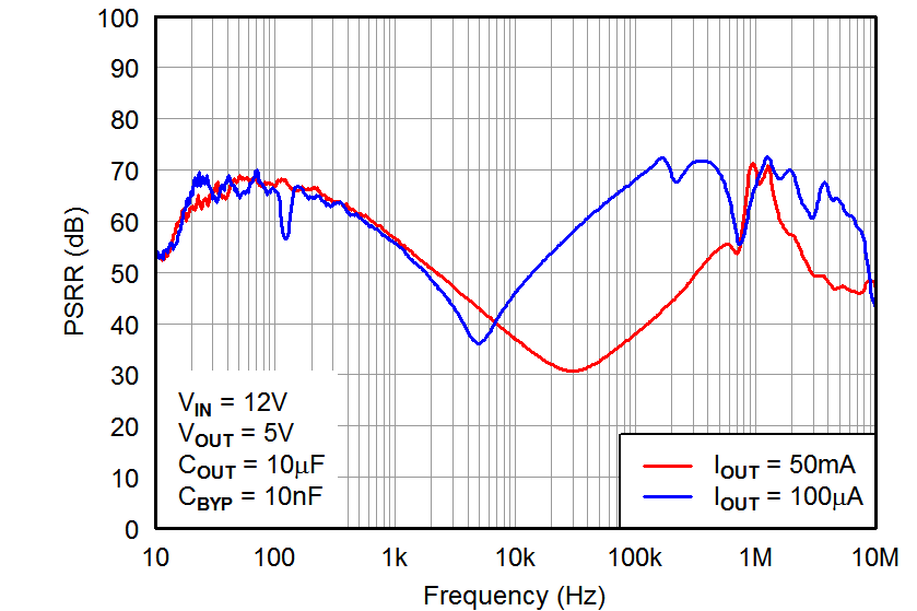
| PSRR | Power-supply rejection ratio | VIN = 12 V, VOUT(NOM) = 5 V, COUT = 10 μF, CBYP(4) = 10 nF, ƒ = 100 Hz | 65 | dB | ||||
| TSD | Thermal shutdown temperature | Shutdown, temperature increasing | 170 | °C | ||||
| Reset, temperature decreasing | 150 | °C | ||||||
| TJ | Operating junction temperature | –40 | 125 | °C | ||||
(1) To ensure stability at no-load conditions, a current from the feedback resistive network greater than or equal to 10μA is required.
(2) Maximum input voltage is limited to 24 V because of the package power dissipation limitations at full load (P ≈ (VIN – VOUT) × IOUT = (24 V – VREF) × 50 mA ≈ 1.14 W). The device is capable of sourcing a maximum current of 50 mA at higher input voltages as long as the power dissipated is within the thermal limits of the package plus any external heatsinking.
(3) IFB > 0 flows out of the device.
(4) CBYP refers to a bypass capacitor connected to the FB and OUT pins.
6.6 Typical Characteristics
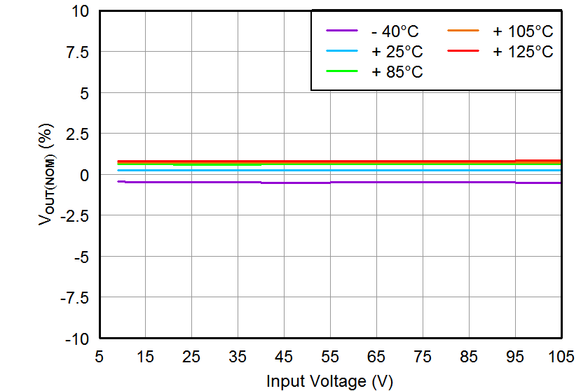
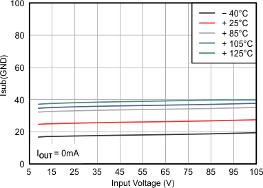
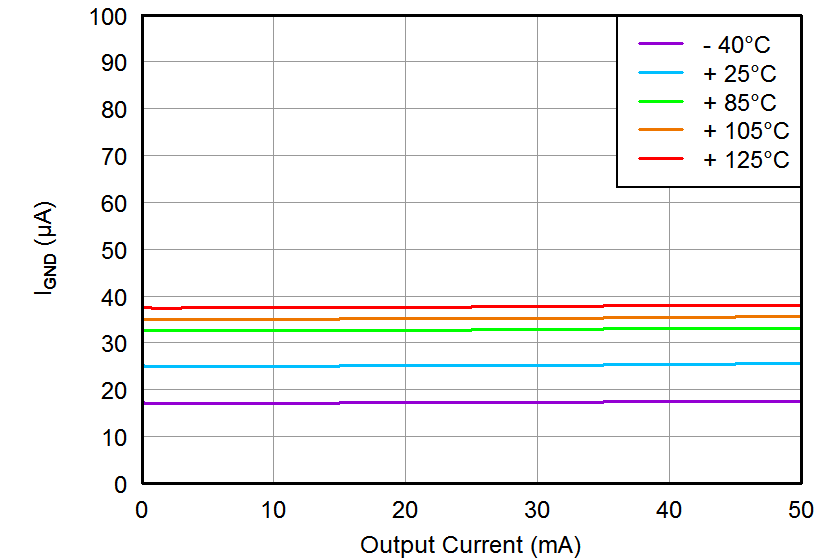
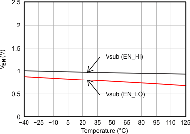
At TJ = –40°C to 125°C, VIN = VOUT(NOM) + 2 V or VIN = 9 V (whichever is greater), VEN = VIN, IOUT = 100 µA, CIN = 1 μF, COUT = 4.7 μF, and FB tied to OUT, unless otherwise noted.
