-
PCM3070 具有嵌入式 miniDSP 的立体声音频编解码器
- 1 特性
- 2 应用
- 3 说明
- 4 LP38690 的
- 5 修订历史记录
- 6 Device Comparison Table
- 7 Pin Configuration and Functions
-
8 Specifications
- 8.1 Absolute Maximum Ratings
- 8.2 Handling Ratings
- 8.3 Recommended Operating Conditions
- 8.4 Thermal Information
- 8.5 Electrical Characteristics, ADC
- 8.6 Electrical Characteristics, Bypass Outputs
- 8.7 Electrical Characteristics, Audio DAC Outputs
- 8.8 Electrical Characteristics, LDO
- 8.9 Electrical Characteristics, Misc.
- 8.10 Electrical Characteristics, Logic Levels
- 8.11 I2S LJF and RJF Timing in Master Mode (see )
- 8.12 I2S LJF and RJF Timing in Slave Mode (see )
- 8.13 DSP Timing in Master Mode (see )
- 8.14 DSP Timing in Slave Mode (see )
- 8.15 I2C Interface Timing
- 8.16 SPI Interface Timing (See )
- 8.17 Typical Characteristics
- 9 Parameter Measurement Information
- 10Detailed Description
- 11Application and Implementation
- 12Power Supply Recommendations
- 13Layout
- 14器件和文档支持
- 15机械封装和可订购信息
- 重要声明
DATA SHEET
PCM3070 具有嵌入式 miniDSP 的立体声音频编解码器
本资源的原文使用英文撰写。 为方便起见,TI 提供了译文;由于翻译过程中可能使用了自动化工具,TI 不保证译文的准确性。 为确认准确性,请务必访问 ti.com 参考最新的英文版本(控制文档)。
1 特性
2 应用
- 条形音箱
- 平板电视
- MP3 坞站
- 蜂窝电话坞站
- 其他立体声或 2.1 家用音频系统
3 说明
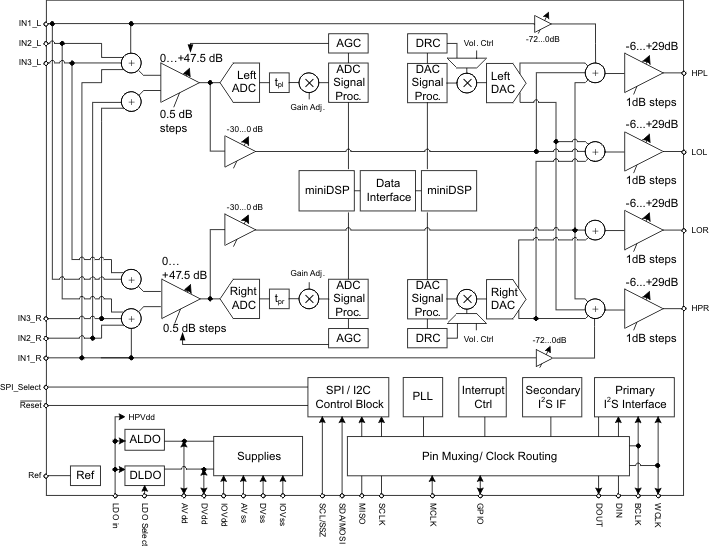
PCM3070 是一款灵活的立体声音频编解码器,配有可编程输入和输出、完全可编程 miniDSP、固定式预定义和可参数化信号处理块、集成式 PLL、集成式 LDO 以及灵活的数字接口。
器件信息(1)
| 器件型号 | 封装 | 封装尺寸(标称值) |
|---|---|---|
| PCM3070 | 超薄四方扁平无引线 (VQFN) (32) | 5.00mm x 5.00mm |
- 要了解所有可用封装,请见数据表末尾的可订购产品附录。
4 LP38690 的

5 修订历史记录
Changes from * Revision (February 2011) to A Revision
- 已添加引脚配置和功能部分,处理额定值表,特性 描述 部分,器件功能模式,应用和实现部分,电源相关建议部分,布局部分,器件和文档支持部分以及机械、封装和可订购信息部分Go
6 Device Comparison Table
| PART NUMBER | DESCRIPTION |
|---|---|
| PCM3070 | Stereo audio codec with embedded miniDSP |
7 Pin Configuration and Functions
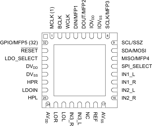
This document describes signals that take on different names depending on how they are configured. In such cases, the different names are placed together and separated by slash (/) characters. For example, "SCL/SS". Active low signals are represented by overbars.
QFN Package
(Bottom View)

Pin Functions
| PIN | NAME | TYPE(1) | DESCRIPTION | |
|---|---|---|---|---|
| 1 | MCLK | DI | Master Clock Input | |
| 2 | BCLK | DIO | Audio serial data bus (primary) bit clock | |
| 3 | WCLK | DIO | Audio serial data bus (primary) word clock | |
| 4 | DIN | DI | Primary function: | |
| Audio serial data bus data input | ||||
| MFP1 | Secondary function: | |||
| General Purpose Clock Input General Purpose Input |
||||
| 5 | DOUT | DO | Primary function: | |
| Audio serial data bus data output | ||||
| MFP2 | Secondary function: | |||
| General Purpose Output Clock Output INT1 Output INT2 Output Audio serial data bus (secondary) bit clock output Audio serial data bus (secondary) word clock output |
||||
| 6 | IOVDD | Power | IO voltage supply 1.1V – 3.6V | |
| 7 | IOVSS | Ground | IO ground supply | |
| 8 | SCLK | DI | Primary function: (SPI_Select = 1) | |
| / | SPI serial clock | |||
| MFP3 | Secondary function: (SPI_Select = 0) | |||
| Audio serial data bus (secondary) bit clock input Audio serial data bus (secondary) DAC or common word clock input Audio serial data bus (secondary) ADC word clock input Audio serial data bus (secondary) data input General Purpose Input |
||||
| 9 | SCL/SS | DI | I2C interface serial clock (SPI_Select = 0) SPI interface mode chip-select signal (SPI_Select = 1) |
|
| 10 | SDA/MOSI | DI | I2C interface mode serial data input (SPI_Select = 0) SPI interface mode serial data input (SPI_Select = 1) |
|
| 11 | MISO | DO | Primary function: (SPI_Select = 1) | |
| / | Serial data output | |||
| MFP4 | Secondary function: (SPI_Select = 0) | |||
| General purpose output CLKOUT output INT1 output INT2 output Audio serial data bus (primary) ADC word clock output Audio serial data bus (secondary) data output Audio serial data bus (secondary) bit clock output Audio serial data bus (secondary) word clock output |
||||
| 12 | SPI_ SELECT | DI | Control mode select pin ( 1 = SPI, 0 = I2C ) | |
| 13 | IN1_L | AI | Multifunction Analog Input, or Single-ended configuration: Line 1 left or Differential configuration: Line right, negative |
|
| 14 | IN1_R | AI | Multifunction Analog Input, or Single-ended configuration: or Line 1 right or Differential configuration: Line right, positive |
|
| 15 | IN2_L | AI | Multifunction Analog Input, or Single-ended configuration: Line 2 left or Differential configuration: Line left, positive |
|
| 16 | IN2_R | AI | Multifunction Analog Input, or Single-ended configuration: Line 2 right or Differential configuration: Line left, negative |
|
| 17 | AVSS | Ground | Analog ground supply | |
| 18 | REF | AO | Reference voltage output for filtering | |
| 19 | NC | -- | NC, do not connect | |
| 20 | IN3_L | AI | Multifunction Analog Input, or Single-ended configuration: Line 3 left, or Differential configuration: Line left, positive, or Differential configuration: Line right, negative |
|
| 21 | IN3_R | AI | Multifunction Analog Input, or Single-ended configuration: Line 3 right, or Differential configuration: Line left, negative, or Differential configuration: Line right, positive |
|
| 22 | LOL | AO | Left line output | |
| 23 | LOR | AO | Right line output | |
| 24 | AVDD | Power | Analog voltage supply 1.5V–1.95V Input when A-LDO disabled, Filtering output when A-LDO enabled |
|
| 25 | HPL | AO | Left high power output driver | |
| 26 | LDOIN/HPVDD | Power | LDO Input supply and Headphone Power supply 1.9V– 3.6V | |
| 27 | HPR | AO | Right high power output driver | |
| 28 | DVSS | Ground | Digital Ground and Chip-substrate | |
| 29 | DVDD | Power | If LDO_SELECT Pin = 0 (D-LDO disabled) | |
| Digital voltage supply 1.26V – 1.95V | ||||
| If LDO_SELECT Pin = 1 (D-LDO enabled) | ||||
| Digital voltage supply filtering output | ||||
| 30 | LDO_ SELECT | DI | D-LDO enable signal (1 = D-LDO enable, 0 = D-LDO disabled) | |
| 31 | RESET | DI | Reset (active low) | |
| 32 | GPIO | DI | Primary function: | |
| General Purpose digital IO | ||||
| MFP5 | Secondary function: | |||
| CLKOUT Output INT1 Output INT2 Output Audio serial data bus ADC word clock output Audio serial data bus (secondary) bit clock output Audio serial data bus (secondary) word clock output |
||||
| Thermal Pad | Thermal Pad | N/A | Connect to PCB ground plane. Not internally connected. | |
(1) DI (Digital Input), DO (Digital Output), DIO (Digital Input/Output), AI (Analog Input), AO (Analog Output), AIO (Analog Input/Output)