• Menu
  • Product
  • Email
  • PDF
  • Order now
  • 300W, 12V Output ZVS Full-Bridge Converter Reference Design for 100kRad Applications

    • TIDT424 March   2025


  • CONTENTS
  • SEARCH
  • 300W, 12V Output ZVS Full-Bridge Converter Reference Design for 100kRad Applications
  1.   1
  2.   Description
  3.   Features
  4.   Applications
  5. 1Test Prerequisites
    1. 1.1 Voltage and Current Requirements
    2. 1.2 Considerations
    3. 1.3 Dimensions
    4. 1.4 Test Setup
  6. 2Testing and Results
    1. 2.1 Efficiency Graphs
    2. 2.2 Efficiency Data
    3. 2.3 Thermal Images
    4. 2.4 Bode Plots
  7. 3Waveforms
    1. 3.1 Switching
    2. 3.2 Output Voltage Ripple
    3. 3.3 Load Transients
    4. 3.4 Start-up Sequence
  8. IMPORTANT NOTICE
search No matches found.
  • Full reading width
    • Full reading width
    • Comfortable reading width
    • Expanded reading width
  • Card for each section
  • Card with all content


Test Report

300W, 12V Output ZVS Full-Bridge Converter Reference Design for 100kRad Applications

Description

This reference design is a full-bridge topology that is comprised of a TPS7H5005-SEP referenced on secondary ground that controls three TPS7H6005-SEP half-bridge gate drivers. The two drivers referenced to the primary side operate in PWM mode which allows for the design to achieve zero-voltage switching (ZVS) at higher loading conditions. On the secondary side the other driver controls a pair of secondary rectifiers to further improve the conversion efficiency. In this design the controller, half-bridge drivers and GaN field-effect transistors (FET) are chosen to meet radiation for geostationary orbit (GEO). These components can be swapped out to meet other mission specifications.

Features

  • GEO class radiation performance
  • GaN FETs on primary and secondary side to increase efficiency
  • Secondary-side controller for faster control loop
  • < 1% voltage ripple on output
  • Single-side assembly, two-layer, 3.25 in × 5.5 in PCB

Applications
  • Command and data handling (C and DH)
  • Optical imaging payload
  • Radar imaging payload
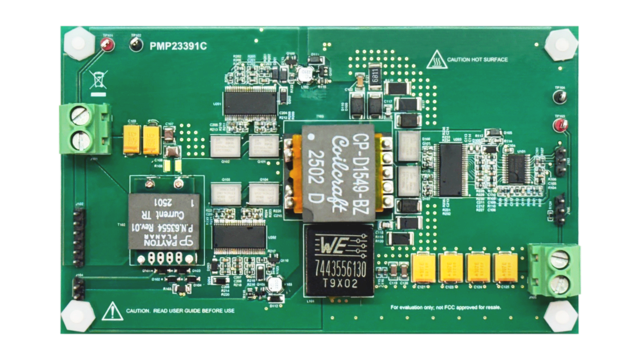
PMP23391 Top of BoardTop of Board
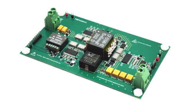
PMP23391 Angled ImageAngled Image
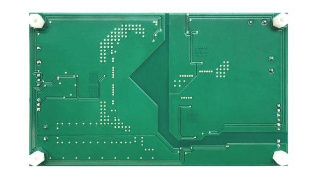
PMP23391 Bottom of BoardBottom of Board


Texas Instruments

© Copyright 1995-2025 Texas Instruments Incorporated. All rights reserved.
Submit documentation feedback | IMPORTANT NOTICE | Trademarks | Privacy policy | Cookie policy | Terms of use | Terms of sale