• Menu
  • Product
  • Email
  • PDF
  • Order now
  • 2.2-W Multi-Output Flybuck Reference Design

    • TIDT312 February   2023


  • CONTENTS
  • SEARCH
  • 2.2-W Multi-Output Flybuck Reference Design
  1.   Description
  2.   Features
  3.   Applications
  4. 1Test Prerequisites
    1. 1.1 Voltage and Current Requirements
  5. 2Testing and Results
    1. 2.1 Efficiency Data
    2. 2.2 Thermal Images
    3. 2.3 Bode Plots
  6. 3Waveforms
    1. 3.1 Switching
    2. 3.2 Output Voltage Ripple
    3. 3.3 Start-Up Sequence
  7. IMPORTANT NOTICE
search No matches found.
  • Full reading width
    • Full reading width
    • Comfortable reading width
    • Expanded reading width
  • Card for each section
  • Card with all content


TEST REPORT

2.2-W Multi-Output Flybuck Reference Design

Description

This reference design is a 2.2-W multi-output flybuck design for isolated gate-drive bias supplies. The supply is designed to accept an input from 24-V systems. This design uses the LM36520 synchronous buck converter to generate four isolated outputs. Primary-side regulation maintains each of the four 17-V outputs within ±10%.

Features

  • Four 17-V isolated outputs
  • Achieves ±10% output voltage accuracy on non-regulated outputs
  • PSR eliminates need for an optocoupler
  • Transformer designed to comply with: IEC61800-5-1

Applications
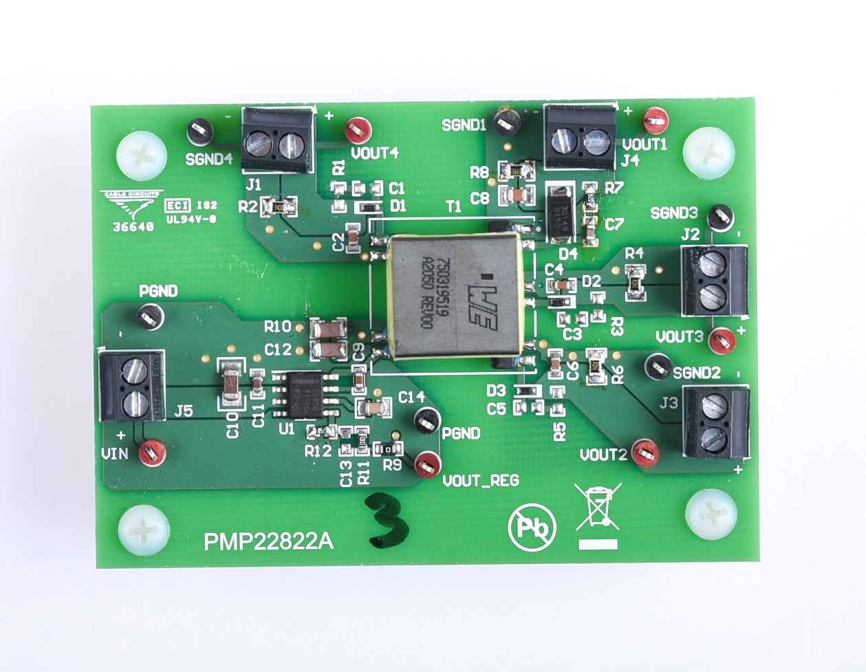
  • Servo drive power supply module

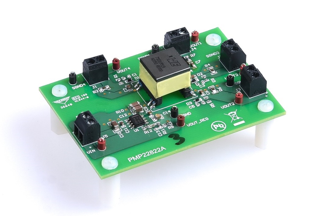
GUID-20230110-SS0I-13NC-ZZZS-W7H84NBCTB3R-low.jpgBoard Top Photo
GUID-20230110-SS0I-7TVD-JMS0-J6VFQBR2DDVJ-low.jpgBottom Side Photo

1 Test Prerequisites


Texas Instruments

© Copyright 1995-2025 Texas Instruments Incorporated. All rights reserved.
Submit documentation feedback | IMPORTANT NOTICE | Trademarks | Privacy policy | Cookie policy | Terms of use | Terms of sale