• Menu
  • Product
  • Email
  • PDF
  • Order now
  • 2-MHz Automotive SEPIC Reference Design

    • TIDT286 June   2022


  • CONTENTS
  • SEARCH
  • 2-MHz Automotive SEPIC Reference Design
  1.   Description
  2.   Features
  3.   Applications
  4. 1Test Prerequisites
    1. 1.1 Voltage and Current Requirements
    2. 1.2 Considerations
    3. 1.3 Dimensions
  5. 2Testing and Results
    1. 2.1 Efficiency Graph
    2. 2.2 Loss Graph
    3. 2.3 Load Regulation
    4. 2.4 Line Regulation
    5. 2.5 Thermal Images
      1. 2.5.1 0.5-A Output Current
      2. 2.5.2 1-A Output Current
      3. 2.5.3 1.5-A Output Current
      4. 2.5.4 2-A Output Current
      5. 2.5.5 Pulsed Ouput Current
    6. 2.6 Bode Plots
      1. 2.6.1 6-V Input Voltage
      2. 2.6.2 12-V Input Voltage
  6. 3Waveforms
    1. 3.1 Switching
      1. 3.1.1 Transistor Q1
        1. 3.1.1.1 Drain - Source
        2. 3.1.1.2 Gate - Source
      2. 3.1.2 Diode D3
    2. 3.2 Input Voltage Ripple
      1. 3.2.1 20-MHz Bandwidth
      2. 3.2.2 Full Bandwidth
    3. 3.3 Output Voltage Ripple
    4. 3.4 Load Transients
      1. 3.4.1 Switching Load From 1 A to 2 A
      2. 3.4.2 Switching Load From 0.2 A to 2 A
        1. 3.4.2.1 50% Duty Cycle
        2. 3.4.2.2 Low Duty Cycle (TON = 3 ms; TOFF = 30 ms)
    5. 3.5 Start-Up Sequence
    6. 3.6 Shutdown Sequence
  7. IMPORTANT NOTICE
search No matches found.
  • Full reading width
    • Full reading width
    • Comfortable reading width
    • Expanded reading width
  • Card for each section
  • Card with all content


TEST REPORT

2-MHz Automotive SEPIC Reference Design

Description

Due to customer demand, this SEPIC converter is designed for 2-MHz switching frequency. Applying such a fairly high switching frequency to a hard switched topology results in increased switching losses at FET and rectifier as well as increased core losses and AC losses at the windings. To minimize those losses the FET and dual inductor must be carefully selected – and by doing so, an efficiency of almost 90% at peak current 2 A by non-synchronous rectification was achieved.

Furthermore, this converter is designed for pulsed load, switching from 0.2 A to 2 A continuously, a current transient of 90%. For best load regulation the loop bandwidth has been tuned achieving a load step response around 1% deviation of output voltage.

Features

  • SEPIC topology is able to step up and step down wide input to output voltage of 12 V
  • Withstands cold cranking as low as 4.5 V and load dump up to 36 VPEAK
  • Due to continuous input current SEPIC topology, low conducted emissions and high switching frequency of 2 MHz were achieved which is beyond the AM broadcast band
  • High switching frequency also provides small inductance to support dynamic loads, means loop bandwidth around 10 kHz results in transient response 1% for 90% load transient
  • The prototype supports as-it-is up to 1.5-A continuous load and up to 2-A pulsed load

Applications
  • Driver monitoring
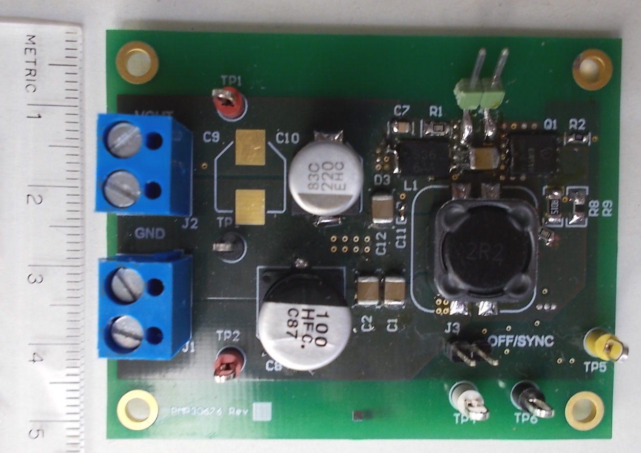
GUID-20220524-SS0I-L50Q-4HHT-PVD0KNXQV3P5-low.jpgTop Photo
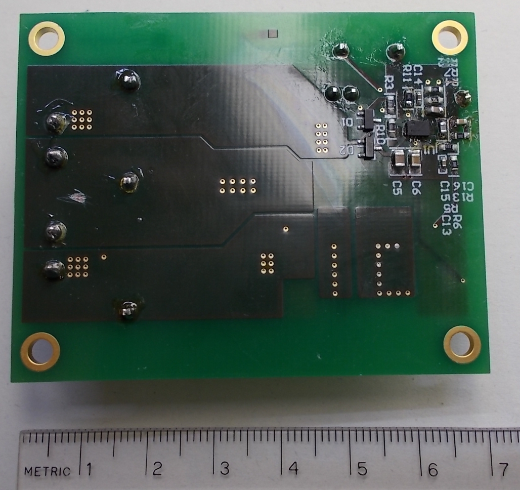
GUID-20220524-SS0I-K3ND-TL9M-2PNBNDHWDFWF-low.jpgBottom Photo


Texas Instruments

© Copyright 1995-2025 Texas Instruments Incorporated. All rights reserved.
Submit documentation feedback | IMPORTANT NOTICE | Trademarks | Privacy policy | Cookie policy | Terms of use | Terms of sale