-
TRF3765 Integer-N/Fractional-N PLL With Integrated VCO
- 1 Features
- 2 Applications
- 3 Description
- 4 Revision History
- 5 Pin Configuration and Functions
- 6 Specifications
- 7 Detailed Description
- 8 Application and Implementation
- 9 Power Supply Recommendations
- 10Layout
- 11Device and Documentation Support
- 12Mechanical, Packaging, and Orderable Information
- IMPORTANT NOTICE
TRF3765 Integer-N/Fractional-N PLL With Integrated VCO
1 Features
- Output Frequencies: 300 MHz to 4.8 GHz
- Low-Noise VCO: –133 dBc/Hz
(1-MHz Offset, fOUT = 2.65 GHz) - 13-/16-Bit Reference/Feedback Divider
- 25-Bit Fractional-N and Integer-N PLL
- Low RMS Jitter: 0.35 ps
- Input Reference Frequency Range:
0.5 MHz to 350 MHz - Programmable Output Divide-by-1/-2/-4/-8
- Four Differential LO Outputs
- External VCO Input with Programmable VCO On/Off Control
2 Applications
- Wireless Infrastructure
- Wireless Local Loop
- Point-to-Point Wireless Access
- Wireless MAN Wideband Transceivers
3 Description
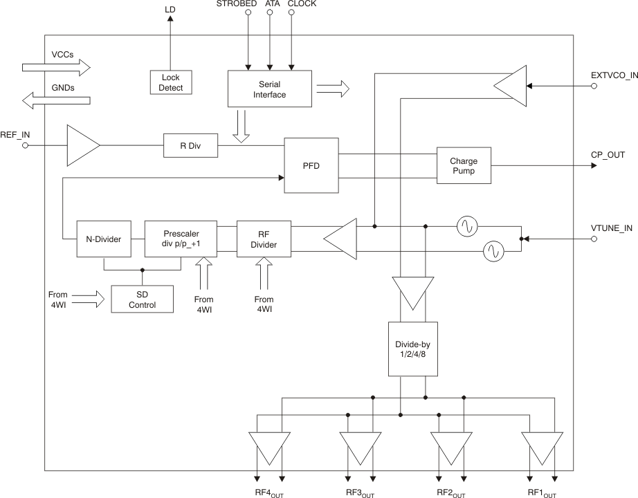
The TRF3765 is a wideband Integer-N/Fractional-N frequency synthesizer with an integrated, wideband voltage-controlled oscillator (VCO). Programmable output dividers enable continuous frequency coverage from 300 MHz to 4.8 GHz. Four separate differential, open-collector RF outputs allow multiple devices to be driven in parallel without the need of external splitters.
The TRF3765 also accepts external VCO input signals and allows on/off control through a programmable control output. For maximum flexibility and wide reference frequency range, wide-range divide ratio settings are programmable and an off-chip loop filter can be used.
The TRF3765 is available in an RHB-32 VQFN package.
Device Information(1)
| PART NUMBER | PACKAGE | BODY SIZE (NOM) |
|---|---|---|
| TRF3765 | VQFN (32) | 5.00 mm x 5.00 mm |
- For all available packages, see the orderable addendum at the end of the datasheet.
Block Diagram

4 Revision History
Changes from D Revision (January 2013) to E Revision
- Added ESD Ratings table, Feature Description section, Device Functional Modes, Application and Implementation section, Power Supply Recommendations section, Layout section, Device and Documentation Support section, and Mechanical, Packaging, and Orderable Information section Go
- Changed Bit27 through Bit30 of Table 7 From: B[25.21] To: B[30..27] Go
Changes from C Revision (December 2011) to D Revision
- Changed the Description of Bit25 and Bit26 in Register 6Go
- Changed the Description of Bit27 and Bit28 in Register 6Go
- Changed the Bit Name of Bit31 From: DIV_MUX_BIAS_OVRT To: DIV_MUX_BIAS_OVRD in Register 6Go
- Changed VCC_OSC From: +3.3V/5.0V To: +3.3V, and VCC_TK From: +3.3V To: +3.3V/5.0V in Go
Changes from B Revision (November 2011) to C Revision
- Changed Reference Oscillator Parameters, Reference input impedance parameter rows in Electrical Characteristics tableGo
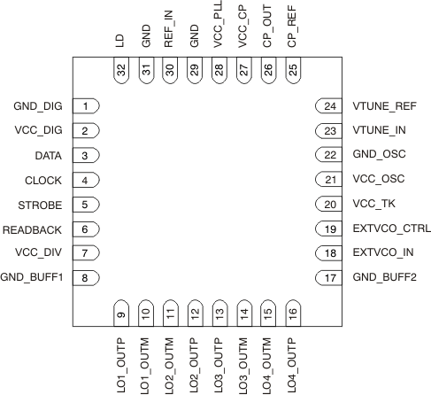
5 Pin Configuration and Functions

Pin Functions
| PIN | I/O | DESCRIPTION | |
|---|---|---|---|
| NO. | NAME | ||
| 4 | CLOCK | I | Serial programming interface, clock input |
| 26 | CP_OUT | O | Charge pump output |
| 25 | CP_REF | — | Charge pump reference ground |
| 3 | DATA | I | Serial programming interface, data input |
| 19 | EXTVCO_CTRL | O | Digital control to enable/disable external VCO |
| 18 | EXTVCO_IN | I | External VCO input |
| 29 | GND | — | Ground |
| 31 | GND | — | Ground |
| 8 | GND_BUFF1 | — | Output buffer ground |
| 17 | GND_BUFF2 | — | Output buffer ground |
| 1 | GND_DIG | — | Digital ground |
| 22 | GND_OSC | — | VCO core ground |
| 32 | LD | O | Lock detector output |
| 10 | LO1_OUTM | O | LO1 output: negative pin |
| 9 | LO1_OUTP | O | LO1 output: positive pin |
| 11 | LO2_OUTM | O | LO2 output: negative pin |
| 12 | LO2_OUTP | O | LO2 output: positive pin |
| 14 | LO3_OUTM | O | LO3 output: negative pin |
| 13 | LO3_OUTP | O | LO3 output: positive pin |
| 15 | LO4_OUTM | O | LO4 output: negative pin |
| 16 | LO4_OUTP | O | LO4 output: positive pin |
| 6 | READBACK | O | Serial programming interface, readback |
| 30 | REF_IN | I | Reference signal input |
| 5 | STROBE | I | Serial programming interface, latch enable |
| 27 | VCC_CP | — | Charge pump power supply |
| 2 | VCC_DIG | — | Digital power supply |
| 7 | VCC_DIV | — | Divider power supply |
| 21 | VCC_OSC | — | VCO core power supply |
| 28 | VCC_PLL | — | PLL power supply |
| 20 | VCC_TK | — | VCO LC tank power supply |
| 23 | VTUNE_IN | — | VCO control voltage |
| 24 | VTUNE_REF | — | VTUNE reference ground |