-
TPS22918 5.5-V, 2-A, 52-mΩ On-Resistance Load Switch
- 1 Features
- 2 Applications
- 3 Description
- 4 Revision History
- 5 Pin Configuration and Functions
- 6 Specifications
- 7 Parameter Measurement Information
- 8 Detailed Description
- 9 Application and Implementation
- 10Power Supply Recommendations
- 11Layout
- 12Device and Documentation Support
- 13Mechanical, Packaging, and Orderable Information
- IMPORTANT NOTICE
TPS22918 5.5-V, 2-A, 52-mΩ On-Resistance Load Switch
1 Features
- Integrated Single Channel Load Switch
- Ambient Operating Temperature: –40°C to +105°C
- Input Voltage Range: 1 V to 5.5 V
- On-Resistance (RON)
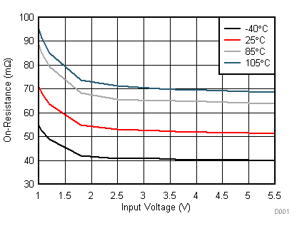
- RON = 52 mΩ (typical) at VIN = 5 V
- RON = 53 mΩ (typical) at VIN = 3.3 V
- 2-A Maximum Continuous Switch Current
- Low Quiescent Current
- 8.3 µA (typical) at VIN = 3.3 V
- Low-Control Input-Threshold Enables Use of 1 V or Higher GPIO
- Adjustable Quick-Output Discharge (QOD)
- Configurable Rise Time With CT Pin
- Small SOT23-6 Package (DBV)
- 2.90-mm × 2.80-mm, 0.95-mm Pitch,
1.45 mm Height (with leads)
- 2.90-mm × 2.80-mm, 0.95-mm Pitch,
- ESD Performance Tested per JESD 22
- ±2-kV HBM and ±1-kV CDM
2 Applications
- Industrial Systems
- Set Top Box
- Blood Glucose Meters
- Electronic Point of Sale
3 Description
The TPS22918 is a single-channel load switch with configurable rise time and configurable quick output discharge. The device contains an N-channel MOSFET that can operate over an input voltage range of 1 V to 5.5 V and can support a maximum continuous current of 2 A. The switch is controlled by an on and off input, which is capable of interfacing directly with low-voltage control signals.
The configurable rise time of the device greatly reduces inrush current caused by large bulk load capacitances, thereby reducing or eliminating power supply droop. The TPS22918 features a configurable quick output discharge (QOD) pin, which controls the fall time of the device to allow design flexibility for power down and sequencing.
The TPS22918 is available in a small, leaded SOT-23 package (DBV) which allows visual inspection of solder joints. The device is characterized for operation over the free-air temperature range of –40°C to +105°C.
Device Information (1)
| PART NUMBER | PACKAGE | BODY SIZE (NOM) |
|---|---|---|
| TPS22918 | SOT-23 (6) | 2.90 mm × 1.60 mm |
- For all available packages, see the orderable addendum at the end of the datasheet.
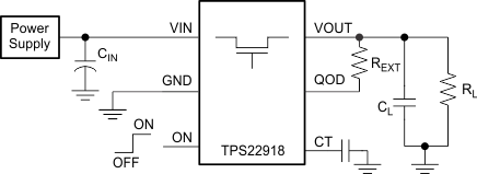
Simplified Schematic
On-Resistance vs Input Voltage
Typical Values
4 Revision History
Changes from A Revision (March 2016) to B Revision
- Updated the constant value in Equation 3 in Adjustable Rise Time (CT) sectionGo
Changes from B Revision (June 2016) to C Revision
- Updated the Applications Section changed µF to pF in Figure 30, Figure 31, and Section 9.2.2.5Go
Changes from * Revision (February 2016) to A Revision
- Changed device status from Product Preview to Production DataGo
5 Pin Configuration and Functions
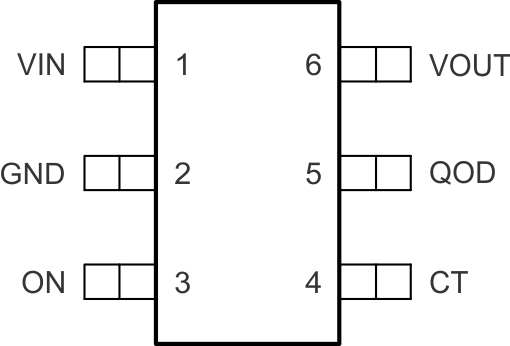
Pin Functions
| PIN | I/O | DESCRIPTION | |
|---|---|---|---|
| NO. | NAME | ||
| 1 | VIN | I | Switch input. Place ceramic bypass capacitor(s) between this pin and GND. See the Detailed Description section for more information. |
| 2 | GND | — | Device ground. |
| 3 | ON | I | Active high switch control input. Do not leave floating. |
| 4 | CT | O | Switch slew rate control. Can be left floating. See the Feature Description section for more information. |
| 5 | QOD | O | Quick Output Discharge pin. This functionality can be enabled in one of three ways.
|
| 6 | VOUT | O | Switch output. |
6 Specifications
6.1 Absolute Maximum Ratings
Over operating free-air temperature range (unless otherwise noted) (1) (2)| MIN | MAX | UNIT | ||
|---|---|---|---|---|
| VIN | Input voltage | –0.3 | 6 | V |
| VOUT | Output voltage | –0.3 | 6 | V |
| VON | ON voltage | –0.3 | 6 | V |
| IMAX | Maximum continuous switch current, ambient temperature = 70°C | 2 | A | |
| IPLS | Maximum pulsed switch current, pulse < 300 µs, 2% duty cycle | 2.5 | A | |
| TJ | Maximum junction temperature | 125 | °C | |
| Tstg | Storage temperature | –65 | 150 | °C |
6.2 ESD Ratings
| VALUE | UNIT | |||
|---|---|---|---|---|
| V(ESD) | Electrostatic discharge | Human-body model (HBM), per ANSI/ESDA/JEDEC JS-001 (1) | ±2000 | V |
| Charged-device model (CDM), per JEDEC specification JESD22-C101 (2) | ±1000 | |||
6.3 Recommended Operating Conditions
Over operating free-air temperature range (unless otherwise noted)| MIN | MAX | UNIT | |||
|---|---|---|---|---|---|
| VIN | Input voltage | 0 | 5.5 | V | |
| VON | ON voltage | 0 | 5.5 | V | |
| VOUT | Output voltage | VIN | V | ||
| VIH, ON | High-level input voltage, ON | VIN = 1 V to 5.5 V | 1 | 5.5 | V |
| VIL, ON | Low-level input voltage, ON | VIN = 1 V to 5.5 V | 0 | 0.5 | V |
| TA | Operating free-air temperature(1) | –40 | 105 | °C | |
| CIN | Input Capacitor | 1 (2) | µF | ||
6.4 Thermal Information
| THERMAL METRIC (1) | TPS22918 | UNIT | |
|---|---|---|---|
| DBV (SOT-23) | |||
| 6 PINS | |||
| RθJA | Junction-to-ambient thermal resistance | 183.2 | °C/W |
| RθJC(top) | Junction-to-case (top) thermal resistance | 151.6 | °C/W |
| RθJB | Junction-to-board thermal resistance | 34.1 | °C/W |
| ψJT | Junction-to-top characterization parameter | 37.2 | °C/W |
| ψJB | Junction-to-board characterization parameter | 33.6 | °C/W |
6.5 Electrical Characteristics
Unless otherwise noted, the specification in the following table applies over the full ambient operating temperature–40°C ≤ TA ≤ +105°C. Typical values are for TA = 25°C.
| PARAMETER | TEST CONDITIONS | TA | MIN | TYP | MAX | UNIT | ||
|---|---|---|---|---|---|---|---|---|
| IQ, VIN | Quiescent current | VON = 5 V, IOUT = 0 A | VIN = 5.5 V | –40°C to +105°C | 9.2 | 16 | µA | |
| VIN = 5 V | 8.7 | 16 | ||||||
| VIN = 3.3 V | 8.3 | 15 | ||||||
| VIN = 1.8 V | 10.2 | 17 | ||||||
| VIN = 1.2 V | 9.3 | 16 | ||||||
| VIN = 1 V | 8.9 | 15 | ||||||
| ISD, VIN | Shutdown current | VON = 0 V, VOUT = 0 V | VIN = 5.5 V | –40°C to +105°C | 0.5 | 5 | µA | |
| VIN = 5 V | 0.5 | 4.5 | ||||||
| VIN = 3.3 V | 0.5 | 3.5 | ||||||
| VIN = 1.8 V | 0.5 | 2.5 | ||||||
| VIN = 1.2 V | 0.4 | 2 | ||||||
| VIN = 1 V | 0.4 | 2 | ||||||
| ION | ON pin input leakage current | VIN = 5.5 V, IOUT = 0 A | –40°C to +105°C | 0.1 | µA | |||
| RON | On-Resistance | VIN = 5.5 V, IOUT = –200 mA | 25°C | 51 | 59 | mΩ | ||
| –40°C to +85°C | 71 | |||||||
| –40°C to +105°C | 78 | |||||||
| VIN = 5.0 V, IOUT = –200 mA | 25°C | 52 | 59 | mΩ | ||||
| –40°C to +85°C | 71 | |||||||
| –40°C to +105°C | 79 | |||||||
| VIN = 4.2 V, IOUT = –200 mA | 25°C | 52 | 59 | mΩ | ||||
| –40°C to +85°C | 71 | |||||||
| –40°C to +105°C | 79 | |||||||
| VIN = 3.3 V, IOUT = –200 mA | 25°C | 53 | 59 | mΩ | ||||
| –40°C to +85°C | 71 | |||||||
| –40°C to +105°C | 80 | |||||||
| VIN = 2.5 V, IOUT = –200 mA | 25°C | 53 | 61 | mΩ | ||||
| –40°C to +85°C | 75 | |||||||
| –40°C to +105°C | 80 | |||||||
| VIN = 1.8 V, IOUT = –200 mA | 25°C | 55 | 65 | mΩ | ||||
| –40°C to +85°C | 79 | |||||||
| –40°C to +105°C | 88 | |||||||
| VIN = 1.2 V, IOUT = –200 mA | 25°C | 64 | 77 | mΩ | ||||
| –40°C to +85°C | 88 | |||||||
| –40°C to +105°C | 104 | |||||||
| VIN = 1.0 V, IOUT = –200 mA | 25°C | 71 | 85 | mΩ | ||||
| –40°C to +85°C | 100 | |||||||
| –40°C to +105°C | 116 | |||||||
| VHYS | ON pin hysteresis | VIN = 1 V to 5.5 V | –40°C to +105°C | 107 | mV | |||
| RPD | Output pull down resistance(1) | VIN = 5.0 V, VON = 0 V | 25°C | 24 | Ω | |||
| –40°C to +105°C | 30 | |||||||
| VIN = 3.3 V, VON = 0 V | 25°C | 25 | ||||||
| –40°C to +105°C | 35 | |||||||
| VIN = 1.8 V, VON = 0 V | 25°C | 45 | ||||||
| –40°C to +105°C | 60 | |||||||
6.6 Switching Characteristics
Refer to the timing test circuit in Figure 21 (unless otherwise noted) for references to external components used for the test condition in the switching characteristics table. Switching characteristics shown below are only valid for the power-up sequence where VIN is already in steady state condition before the ON pin is asserted high. VON = 5 V, TA = 25 °C, QOD = Open.| PARAMETER | TEST CONDITIONS | MIN | TYP | MAX | UNIT | |
|---|---|---|---|---|---|---|
| VIN = 5 V | ||||||
| tON | Turn-on time | RL = 10 Ω, CIN = 1 µF, CL = 0.1 µF, CT = 1000 pF | 1950 | µs | ||
| tOFF | Turn-off time | RL = 10 Ω, CIN = 1 µF, CL = 0.1 µF, CT = 1000 pF | 2 | |||
| tR | VOUT rise time | RL = 10 Ω, CIN = 1 µF, CL = 0.1 µF, CT = 1000 pF | 2540 | |||
| tF | VOUT fall time | RL = 10 Ω, CIN = 1 µF, CL = 0.1 µF, CT = 1000 pF | 2 | |||
| tD | Delay time | RL = 10 Ω, CIN = 1 µF, CL = 0.1 µF, CT = 1000 pF | 690 | |||
| VIN = 3.3 V | ||||||
| tON | Turn-on time | RL = 10 Ω, CIN = 1 µF, CL = 0.1 µF, CT = 1000 pF | 1430 | µs | ||
| tOFF | Turn-off time | RL = 10 Ω, CIN = 1 µF, CL = 0.1 µF, CT = 1000 pF | 2 | |||
| tR | VOUT rise time | RL = 10 Ω, CIN = 1 µF, CL = 0.1 µF, CT = 1000 pF | 1680 | |||
| tF | VOUT fall time | RL = 10 Ω, CIN = 1 µF, CL = 0.1 µF, CT = 1000 pF | 2 | |||
| tD | Delay time | RL = 10 Ω, CIN = 1 µF, CL = 0.1 µF, CT = 1000 pF | 590 | |||
| VIN = 1.8 V | ||||||
| tON | Turn-on time | RL = 10 Ω, CIN = 1 µF, CL = 0.1 µF, CT = 1000 pF | 965 | µs | ||
| tOFF | Turn-off time | RL = 10 Ω, CIN = 1 µF, CL = 0.1 µF, CT = 1000 pF | 2 | |||
| tR | VOUT rise time | RL = 10 Ω, CIN = 1 µF, CL = 0.1 µF, CT = 1000 pF | 960 | |||
| tF | VOUT fall time | RL = 10 Ω, CIN = 1 µF, CL = 0.1 µF, CT = 1000 pF | 2 | |||
| tD | Delay time | RL = 10 Ω, CIN = 1 µF, CL = 0.1 µF, CT = 1000 pF | 480 | |||
| VIN = 1 V | ||||||
| tON | Turn-on time | RL = 10 Ω, CIN = 1 µF, CL = 0.1 µF, CT = 1000 pF | 725 | µs | ||
| tOFF | Turn-off time | RL = 10 Ω, CIN = 1 µF, CL = 0.1 µF, CT = 1000 pF | 3 | |||
| tR | VOUT rise time | RL = 10 Ω, CIN = 1 µF, CL = 0.1 µF, CT = 1000 pF | 560 | |||
| tF | VOUT fall time | RL = 10 Ω, CIN = 1 µF, CL = 0.1 µF, CT = 1000 pF | 2 | |||
| tD | Delay time | RL = 10 Ω, CIN = 1 µF, CL = 0.1 µF, CT = 1000 pF | 430 | |||
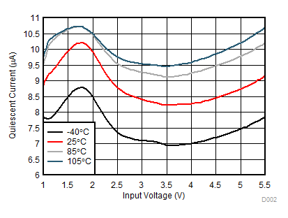
6.7 Typical DC Characteristics
| VON = 5 V | IOUT = 0 A |
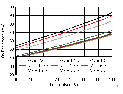
| VON = 5 V | IOUT = –200 mA |
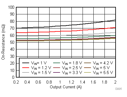
| VON = 5 V | TA = 25°C |
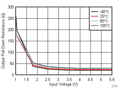
| VIN = VOUT | VON = 0 V |
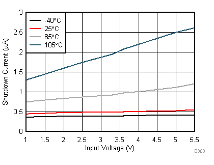
| VON = 0 V | IOUT = 0 A |

| VON = 5 V | IOUT = –200 mA |
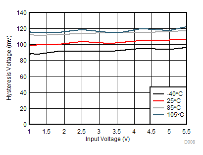
| IOUT = 0 A |
6.8 Typical AC Characteristics
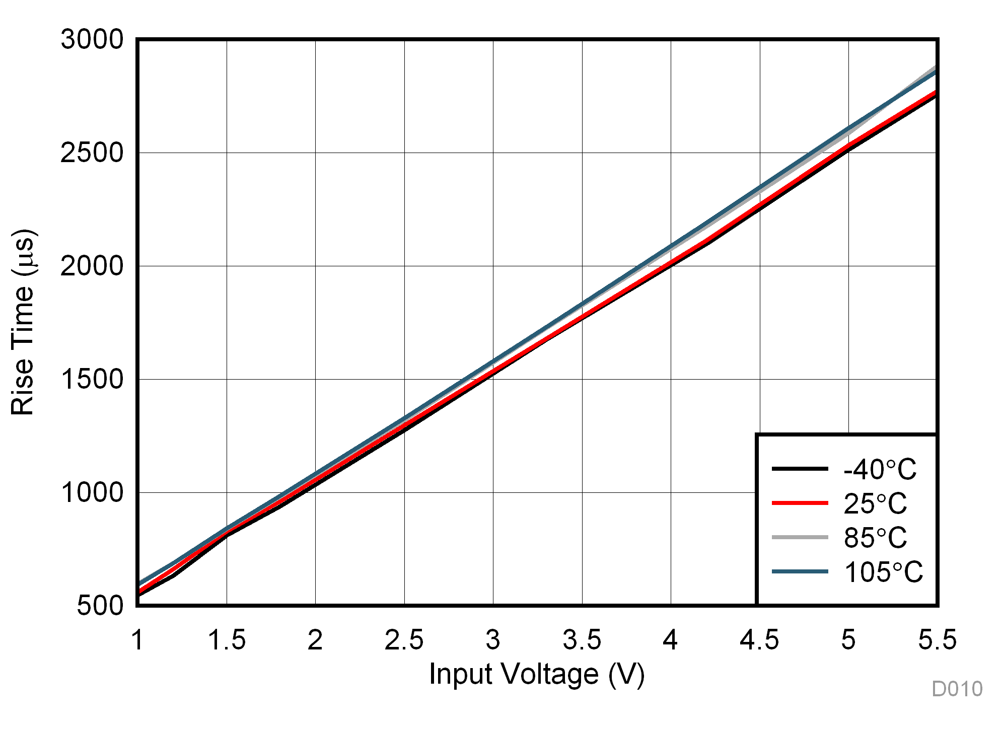
| CIN = 1 µF | RL = 10 Ω | CL = 0.1 µF |
| CT = 1000 pF |
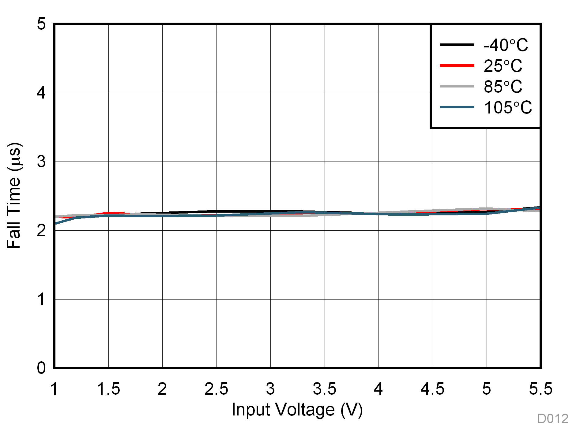
| CIN = 1 µF | RL = 10 Ω | CL = 0.1 µF | QOD = Open |
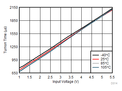
| CIN = 1 µF | RL = 10 Ω | CL = 0.1 µF |
| CT = 1000 pF |
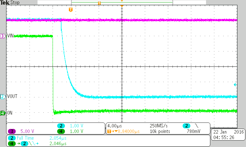
| VIN = 5 V | CIN = 1 µF | CL = 0.1 µF |
| RL = 10 Ω | QOD = Open |
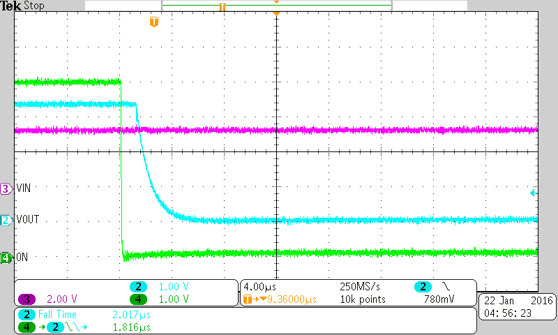
| VIN = 3.3 V | CIN = 1 µF | CL = 0.1 µF |
| RL = 10 Ω | QOD = Open |
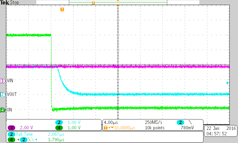
| VIN = 1.8 V | CIN = 1 µF | CL = 0.1 µF |
| RL = 10 Ω | QOD = Open |
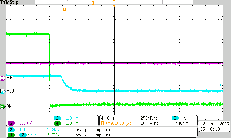
| VIN = 1.0 V | CIN = 1 µF | CL = 0.1 µF |
| RL = 10 Ω | QOD = Open |
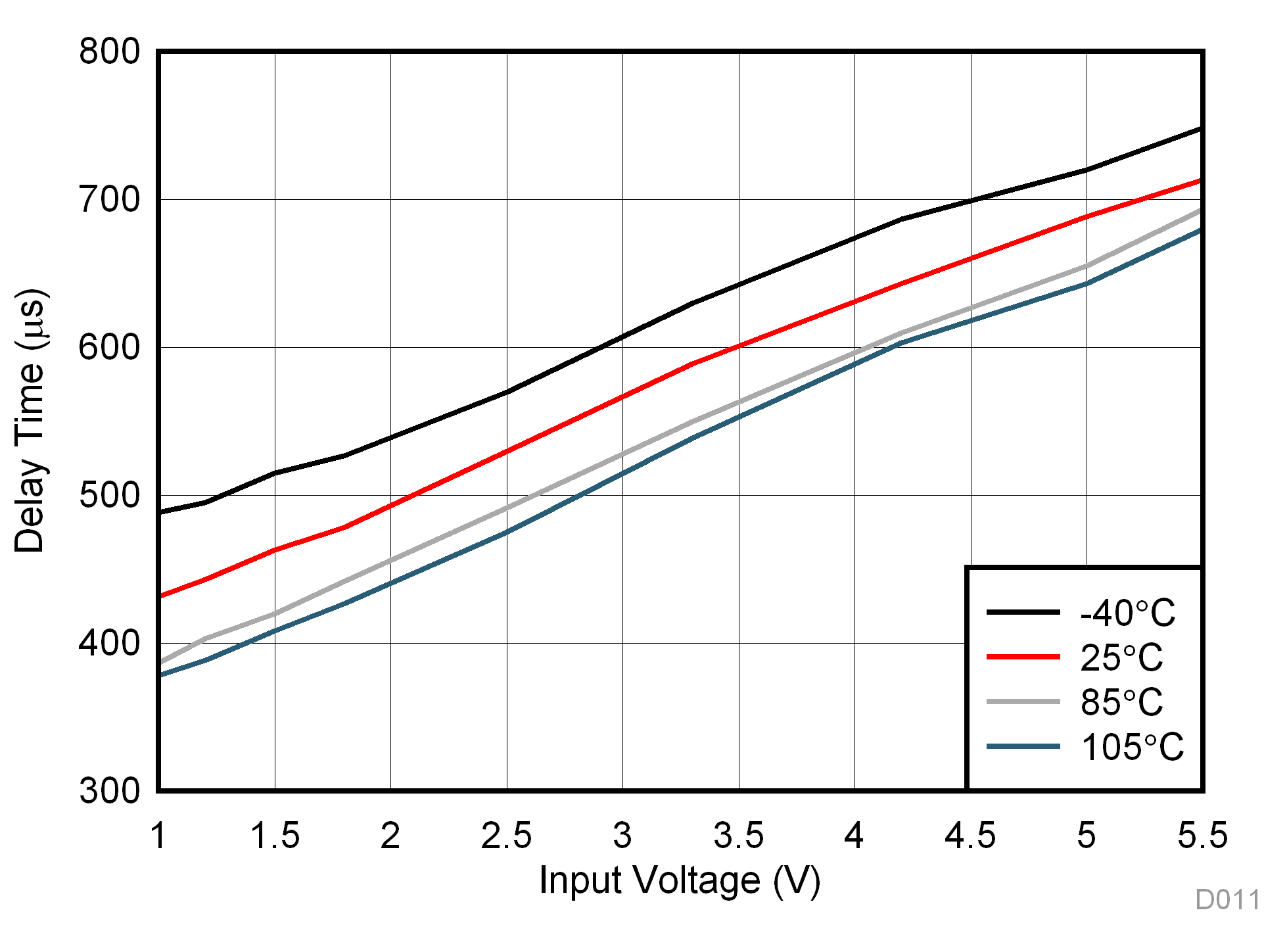
| CIN = 1 µF | RL = 10 Ω | CL = 0.1 µF |
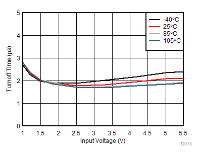
| CIN = 1 µF | RL = 10 Ω | CL = 0.1 µF |
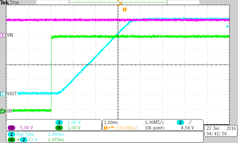
| VIN = 5 V | CIN = 1 µF | CL = 0.1 µF |
| RL = 10 Ω | CT = 1000 pF |
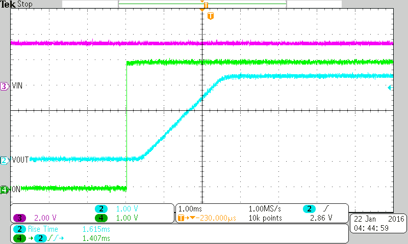
| VIN = 3.3 V | CIN = 1 µF | CL = 0.1 µF |
| RL = 10 Ω | CT = 1000 pF |
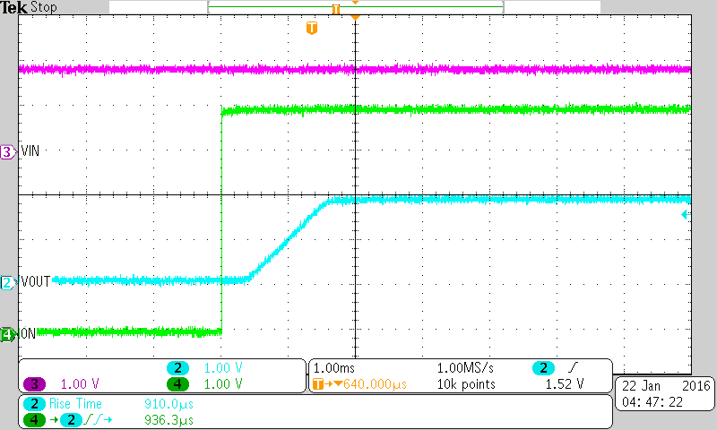
| VIN = 1.8 V | CIN = 1 µF | CL = 0.1 µF |
| RL = 10 Ω | CT = 1000 pF |
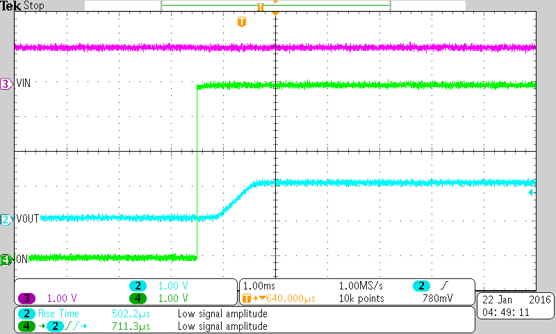
| VIN = 1.0 V | CIN = 1 µF | CL = 0.1 µF |
| RL = 10 Ω | CT = 1000 pF |