-
TPS65270 4.5-V to 18-V Input Voltage, 2-A or 3-A Output Current, Dual Synchronous Step-Down Regulator With Integrated MOSFET
- 1 Features
- 2 Applications
- 3 Description
- 4 Revision History
- 5 Description (continued)
- 6 Pin Configuration and Functions
- 7 Specifications
- 8 Detailed Description
- 9 Application and Implementation
- 10Power Supply Recommendations
- 11Layout
- 12Device and Documentation Support
- 13Mechanical, Packaging, and Orderable Information
- IMPORTANT NOTICE
TPS65270 4.5-V to 18-V Input Voltage, 2-A or 3-A Output Current, Dual Synchronous Step-Down Regulator With Integrated MOSFET
1 Features
- Wide Input Supply Voltage Range: 4.5 V to 18 V
- 0.8 V, ±1% Accuracy Reference
- Up to 2-A (Buck 1) and 3-A (Buck 2) Maximum Continuous Output Loading Current
- Low-Power Pulse Skipping Mode to Achieve High Light Load Efficiency
- Adjustable Switching Frequency
300 kHz to 1.4 MHz Set by External Resistor - Startup With a Prebiased Output Voltage
- Dedicated Enable and Soft Start for Each Buck
- Peak Current-Mode Control With Simple Compensation Circuit
- Cycle-by-Cycle Overcurrent Protection
- 180° Out-of-Phase Operation to Reduce Input Capacitance and Power Supply Induced Noise
- Available in 24-Lead Thermally Enhanced HTSSOP (PWP) and VQFN 4-mm × 4-mm (RGE) Packages
2 Applications
- DTV
- DSL Modems
- Cable Modems
- Set-Top Boxes
- Car DVD Players
- Home Gateway and Access Point Networks
- Wireless Routers
3 Description
The TPS65270 is a monolithic, dual synchronous buck regulator with a wide operating input voltage that can operate in 5-V, 9-V, 12-V, or 15-V bus voltages and battery chemistries. The converters are designed to simplify its application while giving the designer the option to optimize their usage according to the target application.
The TPS65270 features a precision 0.8-V reference and can produce output voltages up to 15 V. Each converter features an enable pin that allows dedicated control of each channel that provides flexibility for power sequencing. Soft-start time in each channel can be adjusted by choosing different external capacitors. TPS65270 is also able to start up with a prebiased output. The converter begins switching when output voltage reaches the prebiased voltage.
Constant frequency peak current-mode control simplifies the compensation and provides fast transient response. Cycle-by-cycle overcurrent protection and hiccup mode operation limits MOSFET power dissipation in short-circuit or overloading fault conditions. Low-side reverse current protection also prevents excessive sinking current from damaging the converter.
Device Information(1)
| PART NUMBER | PACKAGE | BODY SIZE (NOM) |
|---|---|---|
| TPS65270 | HTSSOP (24) | 7.80 mm × 4.40 mm |
| VQFN (24) | 4.00 mm × 4.00 mm |
- For all available packages, see the orderable addendum at the end of the data sheet.
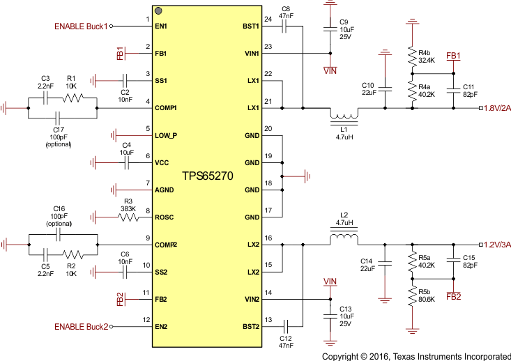
Typical Application

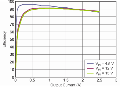
Efficiency vs Output Load

4 Revision History
Changes from D Revision (April 2013) to E Revision
- Added ESD Ratings table, Feature Description section, Device Functional Modes, Application and Implementation section, Power Supply Recommendations section, Layout section, Device and Documentation Support section, and Mechanical, Packaging, and Orderable Information section.Go
- Deleted Ordering Information table; see POA at the end of the data sheetGo
- Changed maximum value of Voltage on VIN1, VIN2, LX1, LX2 from 18 to 20Go
- Changed maximum value of Voltage at LX1, LX2 (maximum withstand voltage transient < 10 ns) from 18 to 23Go
- Changed maximum value of Operating virtual junction temperature, TJ from 125 to 150Go
- Changed Ambient temperature (TA) to Junction temperature (TJ) in Recommended Operating Conditions table and maximum value from 85 to 125Go
- Updated values in the Thermal Information table to align with JEDEC standardsGo
- Changed EN1 and EN2 pin threshold (falling) typical value to maximum value in Electrical Characteristics tableGo
- Changed PSM low power mode threshold (falling) typical value to maximum value in Electrical Characteristics tableGo