-
DRV8832 Low-Voltage Motor Driver IC
- 1 Features
- 2 Applications
- 3 Description
- 4 Revision History
- 5 Pin Configuration and Functions
- 6 Specifications
- 7 Detailed Description
- 8 Application and Implementation
- 9 Power Supply Recommendations
- 10Layout
- 11Device and Documentation Support
- 12Mechanical, Packaging, and Orderable Information
- IMPORTANT NOTICE
DRV8832 Low-Voltage Motor Driver IC
1 Features
- H-Bridge Voltage-Controlled Motor Driver
- Drives DC Motor, One Winding of a Stepper Motor, or Other Actuators/Loads
- Efficient PWM Voltage Control for Constant Motor Speed With Varying Supply Voltages
- Low MOSFET On-Resistance:
HS + LS 450 mΩ
- 1-A Maximum DC/RMS or Peak Drive Current
- 2.75-V to 6.8-V Operating Supply Voltage Range
- 300-nA (Typical) Sleep Mode Current
- Reference Voltage Output
- Current Limit Circuit
- Fault Output
- Thermally-Enhanced Surface Mount Packages
2 Applications
- Battery-Powered:
- Printers
- Toys
- Robotics
- Cameras
- Phones
- Small Actuators, Pumps, and so forth
3 Description
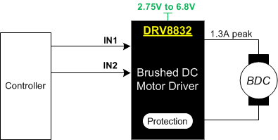
The DRV8832 provides an integrated motor driver solution for battery-powered toys, printers, and other low-voltage or battery-powered motion control applications. The device has one H-bridge driver, and can drive one DC motor or one winding of a stepper motor, as well as other loads like solenoids. The output driver block consists of N-channel and P-channel power MOSFETs configured as an H-bridge to drive the motor winding.
Provided with sufficient PCB heatsinking, the DRV8832 can supply up to 1 A of DC/RMS or peak output current. The device operates on power supply voltages from 2.75 V to 6.8 V.
To maintain constant motor speed over varying battery voltages while maintaining long battery life, a PWM voltage regulation method is provided. An input pin allows programming of the regulated voltage. A built-in voltage reference output is also provided.
Internal protection functions are provided for overcurrent protection, short-circuit protection, undervoltage lockout, and overtemperature protection.
The DRV8832 also provides a current limit function to regulate the motor current during conditions like motor start-up or stall, as well as a fault output pin to signal a host processor of a fault condition.
The DRV8832 is available in a tiny 3-mm × 3-mm 10-pin VSON package and MSOP PowerPAD™ package (Eco-friendly: RoHS & no Sb/Br).
Device Information(1)
| PART NUMBER | PACKAGE | BODY SIZE (NOM) |
|---|---|---|
| DRV8832 | MSOP PowerPAD (10) | 3.00 mm × 3.00 mm |
| VSON (10) | 3.00 mm × 3.00 mm |
- For all available packages, see the orderable addendum at the end of the data sheet.
Simplified Schematic
4 Revision History
Changes from H Revision (October 2013) to I Revision
- Added ESD Ratings table, Feature Description section, Device Functional Modes, Application and Implementation section, Power Supply Recommendations section, Layout section, Device and Documentation Support section, and Mechanical, Packaging, and Orderable Information section Go
- Added VHYS parameter row under the Logic-Level Inputs section in Electrical Characteristics Go
- Changed the paragraph describing the FAULT behavior in Current LimitGo
- Updated the paragraphs in Power Dissipation and added Equation 4Go
5 Pin Configuration and Functions

Pin Functions
| PIN | I/O | DESCRIPTION | ||
|---|---|---|---|---|
| NAME | NO. | |||
| FAULTn | 6 | OD | Fault output | Open-drain output driven low if fault condition present |
| GND | 5 | — | Device ground | |
| IN1 | 9 | I | Bridge A input 1 | Logic high sets OUT1 high |
| IN2 | 10 | I | Bridge A input 2 | Logic high sets OUT2 high |
| ISENSE | 2 | IO | Current sense resistor | Connect current sense resistor to GND. Resistor value sets current limit level. |
| OUT1 | 3 | O | Bridge output 1 | Connect to motor winding |
| OUT2 | 1 | O | Bridge output 2 | Connect to motor winding |
| VCC | 4 | — | Device and motor supply | Bypass to GND with a 0.1-μF (minimum) ceramic capacitor. |
| VREF | 8 | O | Reference voltage output | Reference voltage output |
| VSET | 7 | I | Voltage set input | Input voltage sets output regulation voltage |
6 Specifications
6.1 Absolute Maximum Ratings
over operating free-air temperature range (unless otherwise noted) (1)(2)| MIN | MAX | UNIT | ||
|---|---|---|---|---|
| Power supply voltage, VCC | –0.3 | 7 | V | |
| Input pin voltage | –0.5 | 7 | V | |
| Peak motor drive output current(3) | Internally limited | A | ||
| Continuous motor drive output current(3) | –1 | 1 | A | |
| Continuous total power dissipation | See Thermal Information | |||
| TJ | Operating virtual junction temperature | –40 | 150 | °C |
| Tstg | Storage temperature | –60 | 150 | °C |
6.2 ESD Ratings
| VALUE | UNIT | |||
|---|---|---|---|---|
| V(ESD) | Electrostatic discharge | Human body model (HBM), per ANSI/ESDA/JEDEC JS-001, all pins(1) | ±2500 | V |
| Charged device model (CDM), per JEDEC specification JESD22-C101, all pins(2) | ±1000 | |||
6.3 Recommended Operating Conditions
over operating free-air temperature range (unless otherwise noted)| MIN | NOM | MAX | UNIT | ||
|---|---|---|---|---|---|
| VCC | Motor power supply voltage | 2.75 | 6.8 | V | |
| IOUT | Continuous or peak H-bridge output current(1) | 0 | 1 | A | |
6.4 Thermal Information
| THERMAL METRIC(1) | DRV8832 | UNIT | ||
|---|---|---|---|---|
| DGQ (MSOP PowerPAD) | DRC (VSON) | |||
| 10 PINS | 10 PINS | |||
| RθJA | Junction-to-ambient thermal resistance | 69.3 | 50.2 | °C/W |
| RθJC(top) | Junction-to-case (top) thermal resistance | 63.5 | 78.4 | °C/W |
| RθJB | Junction-to-board thermal resistance | 51.6 | 18.8 | °C/W |
| ψJT | Junction-to-top characterization parameter | 1.5 | 1.1 | °C/W |
| ψJB | Junction-to-board characterization parameter | 23.2 | 17.9 | °C/W |
| RθJC(bot) | Junction-to-case (bottom) thermal resistance | 9.5 | 5.1 | °C/W |
6.5 Electrical Characteristics
VCC = 2.75 V to 6.8 V, TA = –40°C to 85°C (unless otherwise noted)| PARAMETER | TEST CONDITIONS | MIN | TYP | MAX | UNIT | |
|---|---|---|---|---|---|---|
| POWER SUPPLIES | ||||||
| IVCC | VCC operating supply current | VCC = 5 V | 1.4 | 2 | mA | |
| IVCCQ | VCC sleep mode supply current | VCC = 5 V, TA = 25°C | 0.3 | 1 | μA | |
| VUVLO | VCC undervoltage lockout voltage | VCC rising | 2.575 | 2.75 | V | |
| VCC falling | 2.47 | |||||
| LOGIC-LEVEL INPUTS | ||||||
| VIL | Input low voltage | 0.25 × VCC | V | |||
| VHYS | Input hysteresis | 0.08 × Vcc | V | |||
| VIH | Input high voltage | 0.5 × VCC | V | |||
| IIL | Input low current | VIN = 0 | –10 | 10 | μA | |
| IIH | Input high current | VIN = 3.3 V | 50 | μA | ||
| LOGIC-LEVEL OUTPUTS (FAULTn) | ||||||
| VOL | Output low voltage | VCC = 5 V, IOL = 4 mA(1) | 0.5 | V | ||
| H-BRIDGE FETS | ||||||
| RDS(ON) | HS FET on resistance | VCC = 5 V, I O = 0.8 A, TJ = 85°C | 290 | 400 | mΩ | |
| VCC = 5 V, I O = 0.8 A, TJ = 25°C | 250 | |||||
| RDS(ON) | LS FET on resistance | VCC = 5 V, I O = 0.8 A, TJ = 85°C | 230 | 320 | mΩ | |
| VCC = 5 V, I O = 0.8 A, TJ = 25°C | 200 | |||||
| IOFF | Off-state leakage current | –20 | 20 | μA | ||
| MOTOR DRIVER | ||||||
| tR | Rise time | VCC = 3 V, load = 4 Ω | 50 | 300 | ns | |
| tF | Fall time | VCC = 3 V, load = 4 Ω | 50 | 300 | ns | |
| fSW | Internal PWM frequency | 44.5 | kHz | |||
| PROTECTION CIRCUITS | ||||||
| IOCP | Overcurrent protection trip level | 1.3 | 3 | A | ||
| tOCP | OCP deglitch time | 2 | μs | |||
| TTSD | Thermal shutdown temperature | Die temperature(1) | 150 | 160 | 180 | °C |
| VOLTAGE CONTROL | ||||||
| VREF | Reference output voltage | 1.235 | 1.285 | 1.335 | V | |
| ΔVLINE | Line regulation | VCC = 3.3 V to 6 V, VOUT = 3 V(1)
IOUT = 500 mA |
±1% | |||
| ΔVLOAD | Load regulation | VCC = 5 V, VOUT = 3 V IOUT = 200 mA to 800 mA(1) |
±1% | |||
| CURRENT LIMIT | ||||||
| VILIM | Current limit sense voltage | 160 | 200 | 240 | mV | |
| tILIM | Current limit fault deglitch time | 275 | ms | |||
| RISEN | Current limit set resistance (external resistor value) | 0 | 1 | Ω | ||
6.6 Typical Characteristics
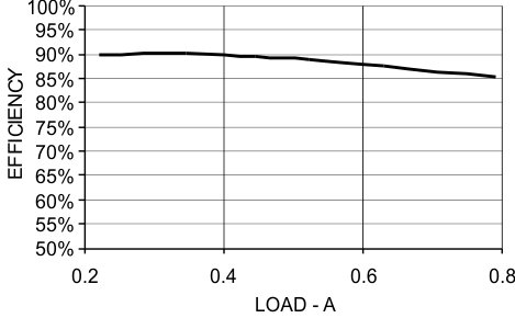
(VIN = 5 V, VOUT = 3 V)
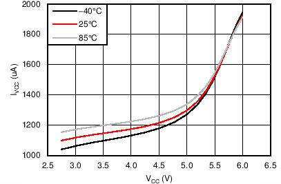 Figure 3. IVCC vs VVCC
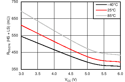 Figure 5. RDS(ON) vs VVCC
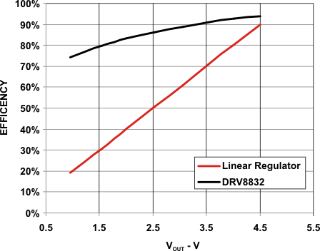 Figure 2. Efficiency vs Output Voltage
(VIN = 5 V, IOUT = 500 mA)
 Figure 4. IVCCQ vs VVCC
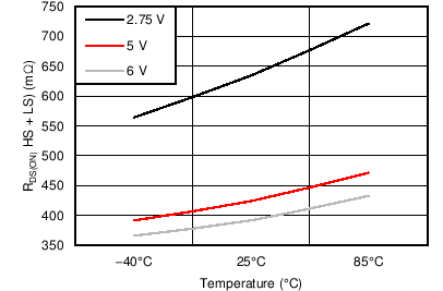 Figure 6. RDS(ON) HS + LS vs Temperature