-
TPS61071-Q1 90% Efficient Synchronous Boost Converter With 600-mA Switch
- 1 Features
- 2 Applications
- 3 Description
- 4 Revision History
- 5 Pin Configuration and Functions
- 6 Specifications
- 7 Detailed Description
- 8 Application and Implementation
- 9 Power Supply Recommendations
- 10Layout
- 11Device and Documentation Support
- 12Mechanical, Packaging, and Orderable Information
- IMPORTANT NOTICE
TPS61071-Q1 90% Efficient Synchronous Boost Converter With 600-mA Switch
1 Features
- Qualified for Automotive Applications
- AEC-Q100 Qualified With the Following Results:
- Device Temperature Grade 2: –40°C to 105°C Ambient Operating Temperature Range
- Device HBM Classification Level 1C
- Device CDM Classification Level C6
- 90% Efficient Synchronous Boost Converter
- 75-mA Output Current at 3.3 V From 0.9-V Input
- 150-mA Output Current at 3.3 V From 1.8-V Input
- Device Quiescent Current: 19 µA (Typical)
- Input Voltage Range: 0.9 V to 5.5 V
- Adjustable Output Voltage Up to 5.5 V
- Power-Save Mode Version Available for
Improved Efficiency at Low Output Power - Load Disconnect During Shutdown
- Overtemperature Protection
- Small 6-Pin Thin SOT Package
2 Applications
- Automotive Power Supplies
- Boost Power Supplies
3 Description
The TPS61071-Q1 device provides a power supply solution for products powered by lower-voltage DC rails or a one-cell, two-cell, or three-cell alkaline, NiCd or NiMH, or one-cell Li-ion or Li-polymer battery. Output currents can go as high as 75 mA, while using a single-cell alkaline, and discharge down to 0.9 V. The device can also generate 5 V at 200 mA from a 3.3-V rail or a Li-ion battery. The boost converter is based on a fixed frequency, pulse-width-modulation (PWM) controller using a synchronous rectifier to obtain maximum efficiency. The maximum peak current in the boost switch is limited typically to a value of 600 mA.
The TPS61071-Q1 output voltage is programmed by an external resistor divider. To minimize battery drain, disable the converter. During shutdown, the load disconnects from the battery. The device package is a 6-pin thin SOT package (DDC).
Device Information(1)
| PART NUMBER | PACKAGE | BODY SIZE (NOM) |
|---|---|---|
| TPS61071-Q1 | SOT (6) | 1.60 mm × 2.90 mm |
- For all available packages, see the orderable addendum at the end of the data sheet.
Typical Application Circuit

4 Revision History
Changes from * Revision (May 2010) to A Revision
- Added ESD Ratings table, Feature Description section, Device Functional Modes, Application and Implementation section, Power Supply Recommendations section, Layout section, Device and Documentation Supportsection, and Mechanical, Packaging, and Orderable Information sectionGo
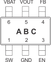
- Changed pinout illustration.Go
- Deleted Dissipation Ratings sectionGo
- Updated Soft Start and Short-Circuit Protection sectionGo
- Updated Device EnablesectionGo
- Changed Figure 20Go
- Updated Inductor Selection sectionGo
5 Pin Configuration and Functions
Pin Functions
| PIN | I/O | DESCRIPTION | |
|---|---|---|---|
| NO. | NAME | ||
| 1 | SW | I | Boost and rectifying switch input |
| 2 | GND | — | Device (IC) ground connection for logic and power |
| 3 | EN | I | Enable input (1/VBAT enabled, 0/GND disabled) |
| 4 | FB | I | Voltage feedback for programming the output voltage |
| 5 | VOUT | O | Boost converter output |
| 6 | VBAT | I | Supply voltage |
