TPS54362-Q1 3-A, 60-V Step-Down DC-DC Converter With Low I(q)
1 Features
- Qualified for Automotive Applications
- AEC-Q100 Qualified With the Following Results:
- Withstands Transients up to 60 V With an Operating Range of 3.6 V to 48 V
- Asynchronous Switch-Mode Regulator With External Components (L and C), Load Current up to 3 A (max.)
- 0.8 V ± 1.5% Voltage Reference
- 200-kHz to 2.2-MHz Switching Frequency
- High-Voltage-Tolerant Enable Input for ON/OFF State
- Soft Start on Enable Cycle
- Slew-Rate Control on Internal Power Switch
- External Clock Input for Synchronization
- Pulse-Skip Mode (PFM) During Light Output Loads With Quiescent Current = 65 μA Typical (LPM Operation)
- External Compensation for Wide-Bandwidth Error Amplifier
- Internal Undervoltage Lockout, UVLO
- Programmable Reset Power-On Delay
- Reset-Function Filter Time for Fast Negative Transients
- Programmable Overvoltage Output Monitoring
- Programmable Undervoltage Output Monitoring, Issuance of Reset if Output Falls Below Threshold
- Thermal Shutdown During Excessive Power Dissipation
- Switch Current-Limit Protection
- Short-Circuit and Overcurrent Protection of FET
- Junction Temperature Range: –40°C to 150°C
- 20-Pin HTSSOP PowerPAD™ Package
- Qualified for Automotive Applications
2 Applications
- Automotive Telematics
- Navigation Systems
- In-Dash Instrumentation
- Battery-Powered Applications
3 Description
The TPS54362-Q1 device is a step-down switch-mode power supply with a low-power mode and a programmable voltage supervisor. Integrated input voltage-line feed-forward topology improves line transient regulation of the voltage-mode buck regulator. The regulator has a cycle-by-cycle current limit. Pulse-skip mode operation under no load reduces the supply current to 65 μA. Using the enable pin reduces the supply shutdown current to 1 μA.
An open-drain reset signal indicates when the nominal output drops below the threshold set by an external resistor-divider network. A soft-start capacitor controls the output voltage start-up ramp. The device activates an internal undervoltage shutdown when the input supply ramps down to 2.6 V.
Frequency foldback operation protects the device during an overload conditions on the output. The device also has thermal shutdown protection due to excessive power dissipation.
The B-revision has an improved leakage current parameter, and improved discharged function while in disable mode.
Device Information(1)
| PART NUMBER | PACKAGE | BODY SIZE (NOM) |
|---|---|---|
| TPS54362-Q1 | HTSSOP (20) | 6.50 mm × 4.40 mm |
- For all available packages, see the orderable addendum at the end of the datasheet.
4 Revision History
Changes from F Revision (May 2014) to G Revision
- Added AEC-Q100 qualification features to the Features section Go
- Added product improvements for B-revision silicon under the Product Description sectionGo
- Increased the max output voltage value for the SS pin in the Absolute Maximum Ratings table Go
- Changed column in Thermal Table from TPS54362A, to TPS54362xGo
- Changed the IIKG row in Elec Chara Table from TPS54362A-Q1 to A-revision and TPS54362B-Q1 to B-revisionGo
- Increased the maximum Ilkg value for both B-revision test conditions in the Electrical Characteristics table Go
- Changed in CAUTION: TPS54362A-Q1 to TPS54362Ax-Q1 and deleted TPS54362B-Q1Go
- Changed in Soft-Start Capacitor paragraph TPS54362A-Q1 to TPS54362Ax-Q1 and deleted TPS54362B-Q1Go
- Changed Power Supply Recommendations section: TPS54362A-Q1 to TPS54362Ax-Q1 and deleted TPS54362B-Q1Go
Changes from E Revision (May 2013) to F Revision
- Changed all text, tables and graphics to the new data sheet template. Go
- Changed pinout drawingGo
- Changed parameter symbols for JEDEC compliance throughout the data sheet Go
- Added a row for the Rslew pin to the Absolute Maximum Ratings tableGo
- Changed symbol for thermal resistance from θ to Rθ in the Thermal Information table Go
- Added Ilkg parameters for EN pin on TPS54362B-Q1 deviceGo
- Revised Figure 22Go
- Changed value of R4 in Output Voltage and Feedback Resistor Selection sectionGo
- Changed several values in the Overvoltage Resistor Selection sectionGo
- Changed several values in the Reset-Threshold Resistor Selection sectionGo
- Changed the voltage value in the Undervoltage Threshold for Low-Power Mode and Load-Transient Operation sectionGo
- Added the TPS54362B-Q1 part number to the text of the Soft-Start Capacitor sectionGo
- Changed calculated values for loop compensation componentsGo
Changes from D Revision (October 2011) to E Revision
- Removed TPS54362-Q1 and TPS54362 from data sheet; added -Q1 to TPS54362A part numbers.Go
- Removed Ordering Information table; see Package Option Addendum for ordering information.Go
- Removed items 3 and 4 from the Soft Start (SS) section, also removed the sentence: Item 3 and item 4 are not applicable for TPS54362A-Q1.Go
- Removed the following sentence from the Soft-Start Capacitor section: Equation 4 has to be satisfied in addition to the other conditions stated in the soft start section of this document (not applicable for TPS54362A-Q1).Go
5 Pin Configuration and Functions
Pin Functions
6 Specifications
6.1 Absolute Maximum Ratings
over operating free-air temperature (unless otherwise noted) (1)6.2 Handling Ratings
| MIN | MAX | UNIT | ||||
|---|---|---|---|---|---|---|
| Tstg | Storage temperature range | –55 | 165 | °C | ||
| V(ESD) | Electrostatic discharge | Human-body model (HBM), per AEC Q100-002(1) | –2 | 2 | kV | |
| Charged-device model (CDM), per AEC Q100-011 | –750 | 750 | V | |||
6.3 Recommended Operating Conditions
over operating free-air temperature (unless otherwise noted)| MIN | MAX | UNIT | ||
|---|---|---|---|---|
| VI | Unregulated buck supply input voltage (VIN, EN) | 3.6 | 48 | V |
| V(VReg) | Regulator voltage range | 0.9 | 18 | V |
| Power up in low-power mode (LPM) or discontinuous mode (DCM) | 0.9 | 5.5 | ||
| Logic level inputs (RST, VSENSE, OV_TH, RST_TH, SYNC, RT) | 0 | 5.25 | V | |
| Logic level inputs (SS, Cdly, COMP) | 0 | 6.5 | V | |
| TJ | Operating junction temperature range(1) | –40 | 150 | °C |
6.4 Thermal Information
| THERMAL METRIC(1) | TPS54362-Q1 | UNIT | |
|---|---|---|---|
| PWP | |||
| 20 PINS | |||
| RθJA | Junction-to-ambient thermal resistance | 43.8 | °C/W |
| RθJC(top) | Junction-to-case (top) thermal resistance | 21.4 | |
| RθJB | Junction-to-board thermal resistance | 18.5 | |
| ψJT | Junction-to-top characterization parameter | 0.5 | |
| ψJB | Junction-to-board characterization parameter | 18.3 | |
| RθJC(bot) | Junction-to-case (bottom) thermal resistance | 1.2 | |
6.5 Electrical Characteristics
V(VIN) = 7 V to 48 V, V(EN) = V(VIN), TJ = –40°C to 150°C (unless otherwise noted)| PARAMETER | TEST CONDITIONS | MIN | TYP | MAX | UNIT | TEST(1) | ||
|---|---|---|---|---|---|---|---|---|
| INPUT POWER SUPPLY | ||||||||
| V(VIN) | Supply voltage on VIN pin | Normal mode–buck mode after initial start-up | 3.6 | 48 | V | Info | ||
| Low-power mode | Falling threshold (LPM disabled) | 8 | V | |||||
| Rising threshold (LPM activated) | 8.5 | |||||||
| High-voltage threshold (LPM disabled) | 25 | 27 | 30 | |||||
| I(q-Normal) | Quiescent current, normal mode | Open-loop test – maximum duty cycle V(VIN) = 7 V to 48 V |
5 | 10 | mA | PT | ||
| I(q-LPM) | Quiescent current; low-power mode | I(VReg) < 1 mA, V(VIN) = 12 V, TA = 25°C | 65 | 75 | μA | PT | ||
| I(VReg) < 1 mA, V(VIN) = 12 V, –40 < TJ < 150°C | 75 | |||||||
| I(VReg) < 1 mA, V(VIN) = 24 V, TA = 25°C | 85 | |||||||
| I(VReg) < 1 mA, V(VIN) = 24 V, –40 < TJ < 150°C | 85 | |||||||
| I(SD) | Shutdown | V(EN) = 0 V, device is OFF, TA = –40°C to 125°C, V(VIN) = 24 V |
10 | μA | PT | |||
| V(EN) = 0 V, device is OFF, TA = 25°C, V(VIN) = 12 V | 1 | 4 | ||||||
| TRANSITION TIMES (LOW-POWER AND NORMAL MODES) | ||||||||
| td(1) | Transition delay from normal mode to low-power mode | V(VIN) = 12 V, V(VReg) = 5 V, I(VReg) = 1 A to 1 mA | 100 | μs | CT | |||
| td(2) | Transition delay from low-power mode to normal mode | V(VIN) = 12 V, V(VReg) = 5 V, I(VReg) = 1 mA to 1 A | 5 | μs | CT | |||
| SWITCH-MODE SUPPLY (VReg) | ||||||||
| V(VReg) | Regulator output | V(VSENSE) = 0.8-V reference | 0.9 | 18 | V | Info | ||
| V(VSENSE) | Feedback voltage | V(VReg) = 0.9 V to 18 V, V(VIN) = 7 V to 48 V | 0.788 | 0.8 | 0.812 | V | CT | |
| rDS(on) | Internal switch resistance | Measured across VIN and PH, I(VReg) = 500 mA | 500 | mΩ | PT | |||
| I(CL) | Switch current limit, cycle-by-cycle | V(VIN) = 12 V | 4 | 6 | 8 | A | Info | |
| t(ON-Min) | Duty-cycle pulse duration (ON) | 50 | 100 | 150 | ns | Info | ||
| t(OFF-Min) | Duty-cycle pulse duration (OFF) | 100 | 200 | 250 | ns | Info | ||
| f(SW) | Switch-mode frequency | Set using external resistor on RT pin | 0.2 | 2.2 | MHz | PT | ||
| Accuracy of f(SW) | –10% | 10% | PT | |||||
| I(Sink) | Sink current in start-up condition | V(OV_TH) = 0 V, V(VReg) = 10 V | 1 | mA | Info | |||
| I(Limit) | Sink-current limit | 0 V < V(OV_TH) < 0.8 V, V(VReg) = 10 V | 80 | mA | Info | |||
| ENABLE (EN) | ||||||||
| VIL | Low input threshold | 0.7 | V | PT | ||||
| VIH | High input threshold | 1.7 | V | PT | ||||
| Ilkg | Leakage into EN pin | A-revision, V(EN) = 60 V | 100 | 135 | μA | PT | ||
| A-revision,, V(EN) = 12 V | 8 | 15 | ||||||
| B-revision, V(EN) = 60 V | 10 | |||||||
| B-revision, V(EN) = 12 V | 2 | |||||||
| RESET DELAY (Cdly) | ||||||||
| IO | External capacitor charge current | V(EN) = high | 1.4 | 2 | 2.6 | μA | PT | |
| VThreshold | Switching threshold | Output voltage in regulation | 2 | V | PT | |||
| LOW-POWER MODE (LPM) | ||||||||
| VIL | Low input threshold | V(VIN) = 12 V | 0.7 | V | PT | |||
| VIH | High input threshold | V(VIN) = 12 V | 1.7 | V | PT | |||
| Ilkg | Leakage into LPM pin | V(LPM) = 5 V | 65 | 95 | μA | PT | ||
| RESET OUTPUT (RST) | ||||||||
| V(RST_TH) | Reset threshold for RST_TH pin | 0.768 | 0.832 | V | PT | |||
| SOFT START (SS) | ||||||||
| I(SS) | Soft-start source current | 40 | 50 | 60 | μA | PT | ||
| SYNCHRONIZATION (SYNC)(2) | ||||||||
| VIL(SYNC) | Low input threshold | 0.7 | V | PT | ||||
| VIH(SYNC) | High input threshold | 1.7 | V | PT | ||||
| Ilkg | Leakage | SYNC = 5 V | 65 | 95 | μA | PT | ||
| Duty(min) | Minimum duty cycle | 30% | CT | |||||
| Duty(miax) | Maximum duty cycle | 70% | CT | |||||
| Rslew | ||||||||
| I(Rslew) | Output current | Rslew = 50 kΩ | 20 | μA | CT | |||
| Rslew = 10 kΩ | 100 | |||||||
| OVERVOLTAGE SUPERVISORS (OV_TH) | ||||||||
| V(OV_TH) | Threshold for OV_TH pin during OV | Internal switch is OFF. | 0.768 | 0.832 | V | PT | ||
| Internal pulldown current on OV_TH pin | OV_TH = 1 V, V(VReg) = 5 V | 70 | mA | |||||
| THERMAL SHUTDOWN | ||||||||
| T(SD) | Thermal shutdown junction temperature | 175 | °C | CT | ||||
| T(HYS) | Temperature hysteresis | 30 | °C | CT | ||||
6.6 Timing Requirements
V(VIN) = 7 V to 48 V, V(EN) = V(VIN), TJ = –40°C to 150°C (unless otherwise noted)| MIN | NOM | MAX | UNIT | TEST(1) | |||
|---|---|---|---|---|---|---|---|
| SYNCHRONIZATION (SYNC)(2) | |||||||
| t(trans-ItoE) | Internal clock to external clock | External clock = 1 MHz, V(VIN) = 12 V, V(VReg) = 5 V |
2.5 | μs | Info | ||
| f(SYNC) | Input clock | V(VIN) = 12 V, V(VReg) = 5 V, f(sw) < f(ext) < 2 × f(sw) |
180 | 2200 | kHz | CT | |
| RESET OUTPUT (RST) | |||||||
| td(POR) | POR delay timer | C2 = 4.7 nF | 3.6 | 7 | ms | PT | |
| td(RSTdly) | Filter time | 10 | 20 | 35 | μs | PT | |
6.7 Switching Characteristics
V(VIN) = 7 V to 48 V, V(EN) = V(VIN), TJ = –40°C to 150°C (unless otherwise noted)| PARAMETER | TEST CONDITIONS | MIN | TYP | MAX | UNIT | TEST(1) | |
|---|---|---|---|---|---|---|---|
| SYNCHRONIZATION (SYNC)(2) | |||||||
| t(trans-EtoI) | External clock to internal clock | Remove external clock, V(VIN) = 12 V, V(VReg) = 5 V | 32 | μs | Info | ||
6.8 Typical Characteristics
6.8.1 Efficiency Data of Power Supply
| V(VIN) = 12 V | V(VReg) = 5 V | f(SW) = 500 kHz |
| L = 22 µH | C4 (output) = 100 µF | TA = 25ºC |
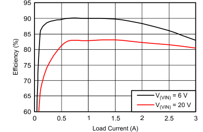
| V(VReg) = 5 V | f(SW) = 500 kHz | L = 22 µH |
| C4 (output) = 100 µF | Rslew = 5 kΩ | TA = 25ºC |
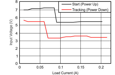
6.8.2 Output Voltage Dropout
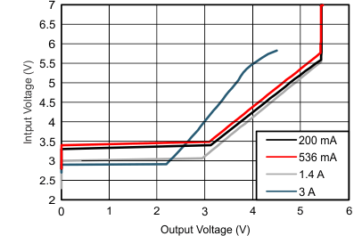
| V(VReg) = 5 V | f(SW) = 500 kHz |
| V(VReg) = 5 V | TA = 25ºC |
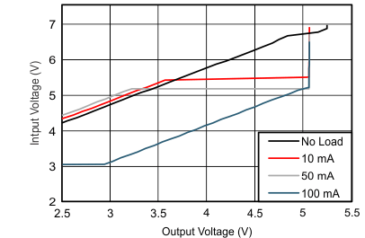
| V(VReg) = 5 V | f(SW) = 500 kHz |
NOTE
Tracking: The input voltage at which the output voltage drops approximately –0.7 V of the regulated voltage or for low input voltages (tracking function) over the load range.
Start: The input voltage required to achieve 5-V regulation on power up with the stated load currents.
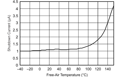
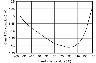
6.8.3 Quiescent and Standby Current
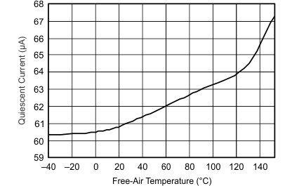
| V(VIN) = 12 V |
| V(VIN) = 12 V |
| EN = High | V(VIN) = 12 V |
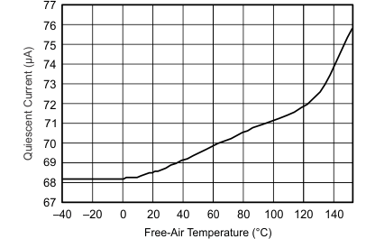
| V(VIN) = 24 V |
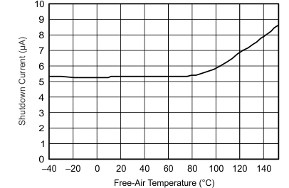
| V(VIN) = 24 V |
6.8.4 Reference Voltages
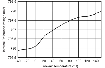
| V(VIN) = 12 V |